 ECEN 204 Electronic Design
Test 1
4 September 2019
ECEN 204 Electronic Design
Test 1
4 September 2019.
Attempt all questions
Closed Book
Total = 75 marks
Time allowed: 90 minutes
Write your answers in the book provided.
Constants
Atomic mass unit
amu
1.66 x 10⁻²⁷ kg
Avogadro’s number
NA
6.02 x 10²³ mol-1
Boltzmann constant
kB
1.38 x 10⁻²³ J.K-1 = 8.62 x 10⁻⁵ eV.K-1
Electron charge
e
1.6 x 10⁻¹⁹ C
Permeability of vacuum
μo
4π x 10-7 H.m-1
Permittivity of vacuum
εo
8.85 x 10⁻¹² F.m-1
Plank’s constant
h
6.626 x 10⁻³⁴ J.s = 4.136 x 10⁻¹⁵ eV.s
Speed of light
c
2.99 x 10⁸ m.s-1
For single crystal silicon:
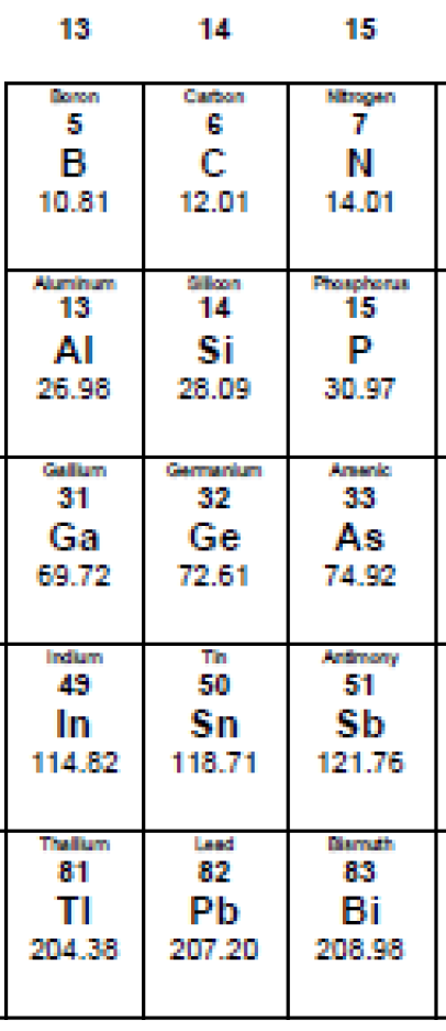
From the periodic table:
Density
ρ = 2.328 g.cm-3
Relative atomic mass = 28.09
Electron mobility =1400 cm2/Vs
e
Hole mobility = 450 cm2/Vs
h
The E12 resistor series:
1.0
1.2
1.5
1.8
2.2
2.7
3.3
3.9
4.7
5.6
6.8
8.2
1
Question 1: Conductivity of solids
20 marks
(a) The band theory of solids can be used to qualitatively explain the difference in electrical
conductivity between metals, semiconductors and insulators. Assume a pure solid with no
impurities added and answer the following questions:
(i) Write down an expression for the electrical conductivity of a solid and explain all your
terms.
(1)
(ii) Use sketches to show how the energy band structure of conductors, semiconductors and
insulators will differ.
(3)
(iii) Now use your answers to (i) and (i ) above and explain the differences in electrical
conductivity between metals, semiconductors and insulators.
(2)
(b) (i) A piece of nichrome wire (a Ni-Cr alloy) has a resistance of 6.5 Ω. The wire has a length
of 10 cm and a diameter of 1.2 mm. Calculate the electrical resistivity of this wire.
(2)
(ii) Explain the potential for measurement errors when measuring very low resistances by
using a standard two-wire multimeter method and explain a method that can be used to
improve the measurement accuracy.
(4)
(c) You must now change the conductivity of a piece of undoped (intrinsic) Si with 1 x 10¹⁰
cm-3 charge carriers to be n-type with a carrier density of ~ 5 x 1015 cm-3.
(i) Explain how this change in carrier concentration can be achieved by impurity doping and
which elements will be most suitable for the doping process. Calculate the ratio of Si to
impurity atoms.
(4)
(iii) Sketch the band structure of this doped semiconductor and explain how this will lead to
a change in carrier concentration.
(2)
(iv) Calculate the expected electrical conductivity for both the undoped and the doped Si in
this question.
(2)
(v) Assume that you have a piece of this doped Si wire with the same dimensions as the NiCr
in Question 1(b). Calculate what the resistance of this Si wire will be.
(2)
2
 Question 2: p-n Junctions and diodes
20 marks
(a)
Question 2: p-n Junctions and diodes
20 marks
(a) (i)
Explain using a sketch or sketches how an electric field will be formed over the
junction between p- and n-semiconductors
. Assume that no bias voltage is applied over the
junction.
(4)
(ii) Sketch the potential energy for both an electron and a hole across this junction.
(2)
(iii) Explain how the electric field across the junction will differ with an applied forward bias
as well as an applied reverse compared to the unbiased case in (i).
(2)
(iv) Explain the movement of charge carriers that will be responsible for producing an
electric current flow under both forward and reverse bias.
(2)
(b) (i) Sketch the approximate diode curve of a real silicon diode in both forward reverse
bias and indicate the typical voltage and currents values that can be expect in significant
regions or points of such a Si diode.
(6)
(ii) Show (sketch) how the behaviour of this real diode in (i) can be modelled as either an
ideal diode or as an ideal diode plus voltage source.
(2)
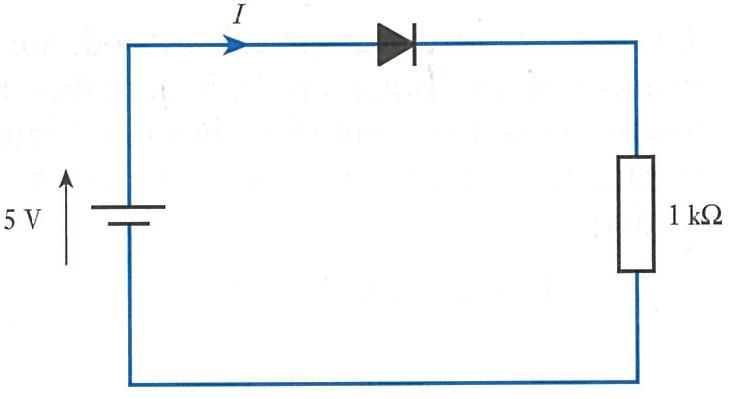
(iii) Use the two different models in (ii) above and calculate voltage drop over the diode as
well as the current through the resistor for each of the two models in the circuit below. (2)
3
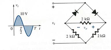
 Question 3: Diode circuits and applications.
35 marks
(a)
Question 3: Diode circuits and applications.
35 marks
(a) You want to use your webcam to take some photographs, but you find that the light level
is too low. To increase the light intensity you decide to place eight white light emitting
diodes around the webcam. You have a 9V DC source to power the LEDs as well as a full E12
series of resistors. According to the LED data sheet you can expect a forward voltage drop of
3.1 V across these diodes and the current should not exceed 30 mA. You have also found
that a current of 20 mA through a diode is ideal to provide the desired light intensity.
(i) Sketch the circuit that you will construct.
(1)
(ii) Calculate the value(s) of any resistor(s) you may use in your circuit.
(2)
(iii) Calculate the total power consumption of your circuit.
(2)
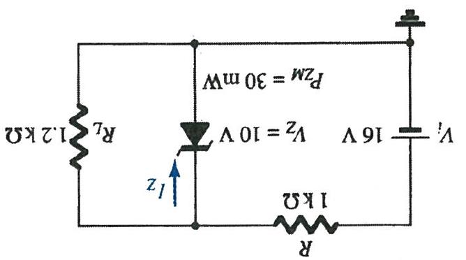
(b) You need to create a voltage reference of ~ 10 V across a load RL = 1.2 kΩ and you come
across this design below on the internet. The Zener diode has a breakthrough value of 10 V
and can dissipate a maximum of 30 mA.
(i) Discuss the merits of this design and show whether the circuit will work or not. [
Hint: Use
the simplest possible model of the Zener diode in your calculations.]
(3)
(ii) Show how the circuit can be modified and improved and calculate the current through
both the Zener and the load.
(3)
(iii) Calculate the power dissipation in the Zener in your new circuit.
(2)
(iv) Assume that the value of RL can be varied. What is the lowest resistance for RL value you
can use for your load for which the modified circuit will function ?
(2)
(iv) Now refine your circuit model of the Zener by including a resistance of 15 Ω and
calculate the actual voltage drop over the load as well as the current through the Zener for
your modified circuit design in (ii).
(3)
4
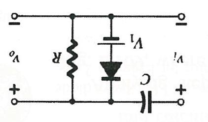 (c)
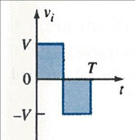
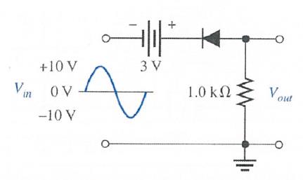
(c) Sketch the output waveform and indicate the expected voltage levels in the circuit
below. Use an ideal diode plus voltage drop model.
(3)
(d) Sketch the output waveform and indicate the expected voltage levels in the circuit
below. Use an ideal diode model.
(3)
+ 10 V
- 10 V
5
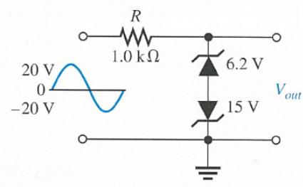
 (d)
(d) Assume that the Zener diodes in the sketch below are ideal Zener diodes, i.e. no internal
resistance. The breakthrough voltage for each of these diodes is indicated in the circuit.
(i) Sketch the output waveform and indicate the voltage levels in the circuit below.
(4)
(ii) Also (on the same time axis) sketch the voltage drop that will be observed over the
resistor.
(2)
(iii) Calculate the peak current that will flow in the circuit.
(2)
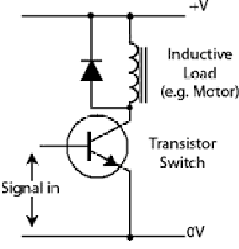
(e) You come across the following circuit, showing an inductive load (such as a relay or small
electric motor) that can be switched on and off by means of a transistor (the Signal in on the
transistor base). Can you explain the use of the diode in this circuit ? What requirement
would be important for this diode ?
(3)
*****
6
 EXAMINATIONS
 –
2019
TRIMESTER 1
ECEN204
ELECTRONIC DESIGN
Time allowed: TWO HOURS
CLOSED BOOK Permitted materials: Only silent non-programmable calculators or silent
programmable calculators with their memories
cleared are permitted in this examination
Non-electronic foreign language to English
dictionaries are permitted.
Instructions:
Answer ALL FIVE questions.
All questions are worth equal marks.
Make use of the constants and useful material
supplied on pages 1 and 2.
Useful material and constants
Constants
Atomic mass unit
amu
1.66 x 10⁻²⁷ kg
Avogadro’s number
NA
6.02 x 10²³ mol-1
Boltzmann constant
kB
1.38 x 10⁻²³ J.K-1 = 8.62 x 10⁻⁵ eV.K-1
Electron charge
e
1.6 x 10⁻¹⁹ C
Permittivity of vacuum
εo
8.85 x 10⁻¹² F.m-1
Plank’s constant
h
6.626 x 10⁻³⁴ J.s = 4.136 x 10⁻¹⁵ eV.s
Speed of light
c
2.99 x 10⁸ m.s-1
ECEN204
Page
1 of
10
 For single crystal silicon:
Density
ρ = 2.328 g.cm-3
Relative atomic mass = 28.09
Electron mobility =1400 cm2/Vs
e
Hole mobility = 450 cm2/Vs
h
From the common emitter BJT small signal model:
mV
25
The internal emitter resistance r
r
e:
e
IE
The total input resistance into the transistor is: R
in(tot) = R1//R2//R
in
The ac input resistance into the base:
R
r
in
ac e
For a MOSFET transistor:
In the non-saturation region:
I
K
V
V V
V
D
n
2
(
2
)
GS
T
DS
DS
In the saturation region:
I
K V
V
D
n
GS
2
t
W
C
k '
W
where
K
n
ox
or
K
n
n
n
2
L
2
L
Other useful formulae:
The E12 resistor series:
1.0
1.2
1.5
1.8
2.2
2.7
3.3
3.9
4.7
5.6
6.8
8.2
ECEN204
Page
2 of
10
 Question 1
Light Emitting Diodes and Solar Cells.
15 marks
(a)
A light emitting diode is manufactured by forming a p-n junction in a semiconductor
material that has an energy gap Eg = 3.1 eV.
(i) Calculate the approximate wavelength of the light that will be emitted by this device.
(1)
(ii) Sketch the expected output spectrum and explain how this may differ from the
wavelength calculated in (i).
(2)
(iii) Explain the operation of white light emitting diodes that are now commonly used as
light bulbs.
(3)
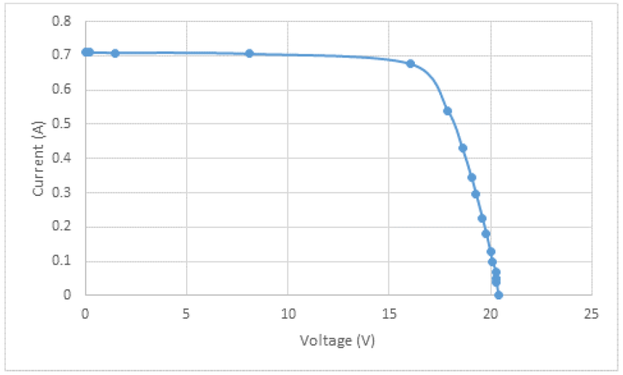
(b) A small crystalline silicon solar module consists of 36 cells, each with an area of 34
mm x 52 mm, that are all connected in series. The module is illuminated with sunlight
of an intensity of 1000 W.m-2 and the current – voltage curve as in the figure below is
obtained.
Use this curve to calculate:
(i) The open circuit voltage and short circuit current.
(2)
(ii) The current and voltage at the maximum power point.
(2)
(iii) The maximum power delivered by the module.
(1)
(iv) The load resistance for maximum power transfer.
(1)
(v) The fill factor of the module.
(1)
(vi) The efficiency of the module.
(2)
ECEN204
Page
3 of
10
Question 2
Bipolar junction transistors
15 marks
a. The three terminals of a bipolar junction transistor are called
(a) p, n, p
(b) n, p, n
(c) input, output, ground
(d) base, emitter, collector
b. For operation as an amplifier, the base of an npn transistor must be
(a) positive with respect to the emitter
(b) negative with respect to the emitter
(c) positive with respect to the collector
(d) 0 V
c. If IC is 50 times larger than IB, then DC is
(a) 0.02
(b) 100
(c) 50
(d) 500
d. If the output of a transistor amplifier is 5 V rms and the input is 100 mV rms, the
voltage gain is
(a) 5
(b) 500
(c) 50
(d) 100
e. To saturate a BJT,
(a) IB = IC(sat)
(b) IB = IC(sat) / DC
(c) VCC must be at least 10 V
(d) the emitter must be grounded
f. The input resistance at the base of a biased transistor depends mainly on
(a) DC
(b) RB
(c) RE
(d) DC and RE
g. In a certain voltage-divider biased npn transistor, VB is 2.95 V. The dc emitter voltage
is approximately
(a) 2.25 V
(b) 2.95 V
(c) 3.65 V
(d) 0.7 V
ECEN204
Page
4 of
10
h. If the dc emitter current in a certain transistor amplifier is 3 mA, the approximate
value of
r’e is
(a) 3 kΩ
(b) 3 Ω
(c) 8.33 Ω
(d) 0.33 kΩ
i. A certain common-emitter amplifier has a voltage gain of 100. If the emitter bypass
capacitor is removed,
(a) the circuit will become unstable
(b) the voltage gain will decrease
(c) the voltage gain will increase
(d) the Q-point will shift
j. A small-signal amplifier
(a) uses only a small portion of its load line
(b) always has an output signal in the mV range
(c) goes into saturation once on each input cycle
(d) is always a common-emitter amplifier
k. For a common-emitter amplifier, RC = 1.0 KΩ, RE = 390 Ω, r’e = 15 Ω, ac = 75.
Assuming that RE is completely bypassed at the operating frequency, the voltage
gain is
(a) 66.7
(b) 2.56
(c) 2.47
(d) 75
l. In the circuit of Question ‘k’, if the frequency is reduced to the point where
XC(bypass) = RE, the voltage gain
(a) remains the same
(b) is less
(c) is greater
m. In a voltage-divider biased npn transistor, if the lower voltage-divider resistor (the
one connected to ground) opens,
(a) the transistor is not affected
(b) the transistor may be driven into cutoff
(c) the transistor may be driven into saturation
(d) the collector current will decrease
n. In a voltage-divider biased pnp transistor, there is no base current, but the base
voltage is approximately correct. The most likely problem(s) is
(a) a bias resistor is open
(b) the collector resistor is open
(c) the base-emitter junction is open
(d) the emitter resistor is open
(e) answers (a) and (c)
(f) answers (c) and (d)
ECEN204
Page
5 of
10
o. In a voltage-divider biased npn transistor, if the upper voltage-divider resistor (the
one connected to VCC) opens,
(a) the transistor goes into cutoff
(b) the transistor goes into saturation
(c) the transistor burns out
(d) the supply voltage is too high
ECEN204
Page
6 of
10
 Question 3
Bipolar junction transistors
15 Marks
Question 3
Bipolar junction transistors
15 Marks
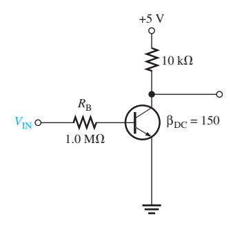
Figure 3.1
a. Determine IC(sat) for the transistor in Figure 3.1. What is the value of IB necessary to
produce saturation? What minimum value of VIN is necessary for saturation?
Assume VCE(sat) = 0 V.
(3)
b. A transistor amplifier has a voltage gain of 50. What is the output voltage when the
input voltage is 100 mV?
(2)
c. A 50 mV signal is applied to the base of a properly biased transistor with r’e = 10
and RC = 560 . Determine the signal voltage at the collector.
(3)
d. Design a biased-transistor circuit using VBB = VCC = 10 V for a Q-point of IC = 5 mA
and VCE = 4 V. Assume DC = 100. The design involves finding RB, RC, and the
minimum power rating of the transistor. (The actual power rating should be greater.)
Sketch the circuit.
(7)
ECEN204
Page
7 of
10
Question 4
MoSFETS
15 Marks
a. A JFET always operates with
(a) the gate-to-source pn junction reverse-biased
(b) the gate-to-source pn junction forward-biased
(c) the drain connected to ground
(d) the gate connected to the source
b. For VGS = 0 V, the drain current becomes constant when VDS exceeds
(a) cutoff
(b) VDD
(c) VP
(d) 0 V
c. In a certain FET circuit, VGS = 0 V, VDD = 15 V, IDSS = 15 mA, and RD = 470 Ω. If RD
is decreased to 330 Ω, IDSS is
(a) 19.5 mA
(b) 10.5 mA
(c) 15 mA
(d) 1 mA
d. A certain JFET datasheet gives VGS(off) = -4 V. The pinch-off voltage, VP,
(a) cannot be determined
(b) is -4 V
(c) depends on VGS
(d) is +4 V
e. For a certain p-channel JFET, VGS(off) = 8 V. The value of VGS for an approximate
midpoint bias is
(a) 4 V
(b) 0 V
(c) 1.25 V
(d) 2.34 V
f. A certain p-channel E-MOSFET has a VGS(th) = -2 V. If VGS is 0 V, the drain current is
(a) 0 A
(b) ID(on)
(c) maximum
(d) IDSS
g. A certain D-MOSFET is biased at VGS = 0 V. Its datasheet specifies IDSS = 20 mA
and VGS(off) is -5 V. The value of the drain current
(a) is 0 A
(b) cannot be determined
(c) is 20 mA
h. An IGBT is generally used in
(a) low-power applications
(b) rf applications
(c) high-voltage applications
(d) low-current applications
ECEN204
Page
8 of
10
i. In a certain common-source (CS) amplifier, Vds = 3.2 V rms and Vgs = 280 mV rms.
The voltage gain is
(a) 1
(b) 11.4
(c) 8.75
(d) 3.2
j. In a certain CS amplifier, RD = 1 KΩ, Rs = 560 Ω, VDD = 10 V and
gm = 4500 µS.
If the source resistor is completely bypassed, the voltage gain is
(a) 450
(b) 45
(c) 4.5
(d) 2.52
k. Ideally, the equivalent circuit of a FET contains
(a) a current source in series with a resistance
(b) a resistance between drain and source terminals
(c) a current source between gate and source terminals
(d) a current source between drain and source terminals
l. The value of the current source in Question ‘k’ is dependent on the
(a) transconductance and gate-to-source voltage
(b) dc supply voltage
(c) external drain resistance
(d) answers (b) and (c)
m. A certain common-source amplifier has a voltage gain of 10. If the source bypass
capacitor is removed,
(a) the voltage gain will increase
(b) the transconductance will increase
(c) the voltage gain will decrease
(d) the Q-point will shift
n. The datasheet for the transistor used in a CD amplifier specifies IGSS = 5 nA at VGS
= 10 V. If the resistor from gate to ground, RG is 50 MΩ, the total input resistance
is approximately
(a) 50 MΩ
(b) 200 MΩ
(c) 40 MΩ
(d) 20.5 MΩ
o. If there is an internal open between the drain and source in a CS amplifier, the drain
voltage is equal to
(a) 0 V
(b) VDD
(c) VGS
(d) VGD
ECEN204
Page
9 of
10
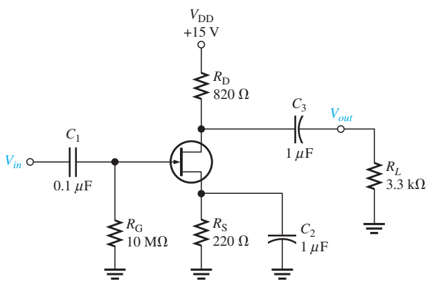 Question 5
MoSFETS
15 Marks
Question 5
MoSFETS
15 Marks
Figure 5.1
a. Determine the drain current in Figure 5.1 given that IDSS = 15 mA and
VGS(off ) = -4 V. The Q-point is centered.
(2)
b. What is the gain of the amplifier in Figure 5.1?
(4)
c. A 4.7 kΩ resistor is connected in parallel with RL in Figure 5.1. What is the voltage
gain?
(2)
d. A JFET has a specified pinch-off voltage of 5 V. When VGS = 0, what is VDS at the
point where the drain current becomes constant?
(2)
e. A certain n-channel JFET is biased such that VGS = -2V. What is the value of
VGS(off) if VP is specified to be 6 V? Is the device on?
(1)
f. A certain JFET datasheet gives VGS(off) = -8 V and IDSS = 10 mA. When VGS = 0,
what is ID for values of VDS above pinch off? VDD = 15 V.
(2)
g. A certain p-channel JFET has a VGS(off) = 6 V. What is ID when VGS = 8 V?
(2)
******************
ECEN204
Page
10 of
10
EEEN 204 Electronic Design
Test 1
4 September 2023
Name: ………………………………………………………………………
Student Number:……………………………………………………….
Instructions
Attempt all questions
Time: 5 minutes for reading test + 50 minutes writing time.
Total = 50 marks
Write your answers in the spaces provided. An extra sheet is supplied at the back if more
space should be needed.
You are allowed one double sides A4 sheet with your own notes during the test.
Assume that you are working with silicon unless a different material is specified.
Test starts on page 4
Question
Marks
Achieved
1 – Semiconductors
18
and pn junctions
3 – Diodes and
18
diode circuits
4 – Transistors
14
Total
50
1
 Some potentially useful constants and material properties
Atomic mass unit
amu
1.66 x 10⁻²⁷ kg
Avogadro’s number
NA
6.02 x 10²³ mol-1
Boltzmann constant
k or kB
1.38 x 10⁻²³ J.K-1 = 8.62 x 10⁻⁵ eV.K-1
Electron charge
e
1.6 x 10⁻¹⁹ C
Permeability of vacuum
μo
4π x 10-7 H.m-1
Permittivity of vacuum
εo
8.85 x 10⁻¹² F.m-1
Plank’s constant
h
6.626 x 10⁻³⁴ J.s = 4.136 x 10⁻¹⁵ eV.s
Speed of light
c
2.99 x 10⁸ m.s-1
For single crystal silicon:
Density
ρ = 2.328 g.cm-3
Relative atomic mass = 28.09
Electron mobility =1400 cm2/Vs
e
Hole mobility = 450 cm2/Vs
h
Energy gap Eg = 1.1 eV
Intrinsic carrier concentration at 300 K = 1 x 1010 cm-3
From Periodic Table:
2
An expression for the intrinsic carrier concentration in a semiconductor is given by:
E
2
g
np =
n =
N N exp
i
c
v
−
kT
Where Nc and Nv are the so-called density of states. For Si (Eg = 1.1 eV) these values can be
calculated as:
Nc = (5.41 x 10¹⁵)*T3/2
Nv = (2.23 x 10¹⁵)*T3/2 where T is the temperature in Kelvin.
The E12 resistor series:
1.0
1.2
1.5
1.8
2.2
2.7
3.3
3.9
4.7
5.6
6.8
8.2
For transistors, unless otherwise stated, you should assume VDD = 5.0 V and that:
For nMOS devices
Vt = 1.0 V
Vtd = -3.0 V
For pMOS devices
Vtp = -1.0 V Vtpd = 3.0 V
𝛽
2
For FETS in saturation, Ids = (V
2
gs − Vt)
2
(V − V
gs
t )
V
In non-saturation I
V −
ds
ds =
ds
2
3
Question 1 Semiconductors and pn junctions
[18]
(a) Silicon is doped with As atoms to a concentration of 1 x 1016 cm-3. Calculate the
resultant:
(i) concentration electrons in the Si
(2)
(ii) concentration of holes in the Si
(2)
(iii) electrical conductivity of the Si.
(2)
(iv) Explain any changes in the magnitude of the Si bandgap that you would expect as a
result of the doping process.
(2)
4
(b) A p-n junction is formed between p-type Si with an acceptor density of 5 x 1016 cm-3 and
n-type Si with a donor density of 5 x 1015 cm-3. No bias voltage is applied to this junction.
Sketch a cross section of this structure in equilibrium and indicate all charged species in this
structure and whether these charges are mobile or static. Also indicate the direction of the
electric field and the relative width of the depletion region.
(6)
(ii) Explain how the electric field across the junction and the width of the depletion region
will change under an applied forward bias and a reverse bias
(4)
5
 Question 3 Diodes properties and circuits
[18]
(a)
Question 3 Diodes properties and circuits
[18]
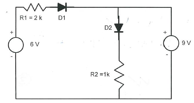
(a) Model the diodes in the circuit below as ideal diodes and calculate the current through
each diode and the voltage drop over each of the diodes.
(5)
6
 (b)
(b) You must design a voltage reference based on a Zener diode that is capable of driving a
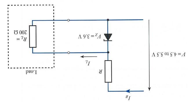
fixed 200 Ω load. This supply voltage can vary from 4.5 to 5.5 V as shown in the figure
below. In order to limit the power dissipation in your circuit, you want to make the value of
R as high as possible.
Calculate:
(i) The maximum value for the resistor R that will ensure the circuit will still function as
intended.
(4)
(ii) The maximum power dissipation in the Zener diode.
(3)
7
 (c) (i)
 Explain the role of each of the two diodes in the circuit below
(2)
(ii) Sketch the shape and magnitude of the expected output waveform for the circuit below.
Use an ideal diode plus voltage drop model for your calculations.
(4)
8
Question 4 - Transistors
[14]
(a) What two conditions are required for current to flow between the source and the drain of
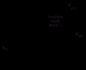
an nMOS depletion mode transistor? Express your answer in terms of Vgs, Vds and Vtd.
(2)
(b) What two conditions are required for a pMOS enhancement mode transistor to be
operating in its saturation mode? Express your answer in terms of Vgs, Vds and Vtp.
[2]
(c) Sketch a two input NAND gate using only nMOS enhancement and depletion mode
transistors.
(3)
9
(d)
Derive an expression for the steady state
output current of the NAND gate designed in (c)
above, if its output was connected to an identical NAND gate.
(1)
(e) Draw the block diagram for a CMOS transistor clearly illustrating all the layers. (2)
10
(f) An nMOS enhancement mode transistor has a of 20 mA/V2. When operating in its
saturated mode, what gate voltage (Vgs) is required in order for the drain-source current (Ids) to
reach 90 mA ? Assume the supply and threshold voltages provided at the beginning of this
test.
(4)
*****End of Test*****
11
12
13
EEEN 204 Electronic Design
Test 2
23 October 2024
Name: ………………………………………………………………………
Student Number:……………………………………………………….
Instructions
Attempt all questions
Time: 120 minutes
Total = 100 marks
Write your answers in the spaces provided. An extra sheet is supplied at the back if
more space should be needed.
You are allowed one double sided A4 sheet with your own notes during the test.
Assume that you are working with silicon unless a different material is specified.
Test starts on page 3
Question
Marks
Achieved
1 – Diodes and
25
diode circuits
2 – MOSFETS
45
4 – BJTs
30
Total
100
1
Some potentially useful information
The E12 resistor series:
1.0
1.2
1.5
1.8
2.2
2.7
3.3
3.9
4.7
5.6
6.8
8.2
For MOSFET transistors, unless otherwise stated, you should assume VDD = 5.0 V and
that:
For nMOS devices
Vt = 1.0 V
Vtd = -3.0 V
For pMOS devices
Vtp = -1.0 V Vtpd = 3.0 V
𝛽
2
For FETS in saturation:
Ids = (V
2
gs − Vt)
2
(V − V
gs
t )
V
In
ds
non-saturation:
I
V −
ds =
ds
2
The question referring to switch logic, has a threshold voltage for these pass transistors of 0.5 V
2
 Question 1: Diodes properties and circuits
[25 marks]
(a)
Question 1: Diodes properties and circuits
[25 marks]
(a) Model the diodes in the circuit below as ideal diodes and calculate the current through
each diode and the voltage drop over each of the diodes.
(5)
3
 (b)
(b) You must design a voltage reference based on a Zener diode that is capable of driving a
fixed 200 Ω load. This supply voltage can vary from 4.5 to 5.5 V as shown in the figure
below. In order to limit the power dissipation in your circuit, you want to make the
value of R as high as possible.
Calculate:
(i)
The maximum value for the resistor R that will ensure the circuit will still function as
intended.
(5)
(ii)
The maximum power dissipation in the Zener diode.
(5)
4
(c)
(10 marks total)
(i)
Sketch the arrangements of diodes you will use to create a full-wave bridge rectifier.
Include the load resistor in your circuit and clearly show where the output voltage will
be obtained.
(3)
(ii)
An AC signal is now connected as the input to your bridge rectifier. You have measured
the voltage of this input signal and your multimeter has indicated a voltage of 10.61 V.
Sketch the output signal and indicate the maximum voltage level of the signal. Model
your diodes as ideal diodes with a voltage drop (0.7V).
(3)
5
(iii) Explain how your output in
(ii) above can be smoothed to obtain a more stable output
voltage (not regulated yet).
Sketch any changes you will make to your basic circuit in
(i) and calculate an approximate value for any components that you add.
For this
calculation assume that your load resistance has a value of 1 kΩ.
(3)
(iv) Instead of the AC signal in (ii), a DC voltage source of 20V is now accidently connected
to the input of your diode bridge. Explain how this will change the expected output
signal and voltage levels.
(1)
6
Question 2: MOSFETs
[45 marks]
(a)
Draw the schematic diagram of a pMOS inverter that uses one pMOS enhancement mode
and one pMOS depletion mode transistor. The depletion mode inverter should have a L:W
ratio of 4 times that of the enhancement mode (i.e. a 4:1 inverter).
(3)
(b)
Derive an expression for the steady state
output current of the inverter gate designed in
(a)
above, if its output was connected to an identical inverter.
(1)
(c)
What
two conditions are required for a
pMOS enhancement mode transistor to be operating
in its
saturated mode?
(3)
7
(d)
Draw the block diagram for a CMOS transistor clearly illustrating all the layers.
(2)
(e)
Draw the schematic diagram of a two-input CMOS NAND gate.
(3)
(f)
Draw the schematic diagram of a two-input, 4:1 pMOS NAND gate using only pMOS
enhancement mode and depletion mode transistors.
(5)
8
(g)
What are the two most significant reasons that FETs are used in high density (VLSI) circuits
rather than BJTs?
(2)
(h)
For the pass transistor circuit below, the threshold voltage is 0.5 V, inputs A, B and C are at
VDD = 5.0 V, as are the gate voltages at D. What is the resulting voltage at point Y? Show your
working.
(2)
D = 5.0 V
A
B
C
Y
9
 (i)
(i)
Calculate the voltage swing of a standard nMOS
inverter (one enhancement mode and one depletion
mode transistor as on the right) where the pull-up
(depletion transistor) has a L:W ratio of
6:1, and the
pull-down (enhancement mode transistor) has a L:W
ratio of
1:1. This is a 6:1 inverter. You may assume
that Vin(low) is < Vt, and Vin(high) is VDD.
(4 marks)
10
 (j)
(j)
What is the minimum pull-up:pull-down (Zpu:Zpd) ratio that is
required to ensure that Vout (logic low) would turn off the input
transistor of an identical inverter? I.e., what Zpu:Zpd would
ensure that Vout (low) < Vtn?
(8 marks)
11


 (k)
(k)
For the circuit on the right, determine if the nMOSFET is
VDD = 12 V
in saturation mode and find the drain current ID. The
transistor has a threshold voltage Vt = 2 V and
= 2 mA/V2.
ID
3.6 k
6.0 M
(12 marks)
4.0 M
820
ID
12
 Question 3: BJTs
[30 marks]
(a)
Question 3: BJTs
[30 marks]
(a) Determine to 2 decimal places, α and β for a BJT given an emitter current of 6.602 mA and a
base current of 60 µA.
(2)
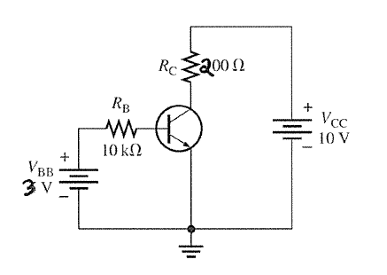
(b) Determine IB, IC, IE, VCE and VCB for the circuit on the right if
βDC = 50, RC = 200 and VBB = 3 V.
(4 marks)
13
(c)
What two conditions are required for an NPN transistor to be operating in its active region?
(2)
(d)
Is the NPN transistor of question (b) above, operating in its cutoff, active, or saturation
mode? Show your working.
(2)
(e)
Would a bipolar or a MOSFET transistor be more radiation
immune?
Briefly explain your
answer.
(3)
14
 (f)
(f)
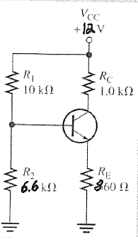
Referring to the circuit on the right:
(4 marks total)
(i)
What is the purpose of the resistors R1 and R2?
(2)
(ii)
What is the purpose of the resistor RE?
(2)
15
 (g)
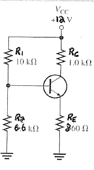
(g)
Determine VCE and IC in the stiff voltage-divider based circuit on the
right if βDC = 50, R2 = 6.6 k, RE = 860 and VCC = 12 V.
If you need to assume the device is in active mode, ensure you
check your results to confirm this assumption. Show evidence of
this confirmation.
(
7 marks)
16
(h)
Detail the most significant advantage AND the most significant disadvantage of using a
class B amplifier over a class A amplifier.
(2)
(i)
Sketch a simple circuit that would operate as an inverting switch using one NPN
transistor and 2 resistors.
(2)
(j)
Would the transistor in your circuit designed in
(i) above, ideally be operating in its
cutoff, active or saturated mode? Briefly explain.
(2)
*****End of Test*****
17
18
19
20
Document Outline