EEEN313 Test 1
Time Allowed: Two hours
Instructions: Answer ALL questions on the paper provided and show working where
possible. There are 14 questions, of which 10 are multiple choice.
It is essential all answers given are your own, you must not work with anyone else
during the test
For the multiple choice questions, circle the letter that corresponds to the answers that
you believe are correct (there can be more than one correct answer for each question)
Potentially useful formulas, datasheets and additional working space can be found at
the end of this test.
Student name:
Student number:
Multiple Choice (20 points)
1. (2 points) Which of the following answers best describes discontinuous conduction mode?
A. The inductor voltage ripple goes negative
B. The inductor current ripple stays positive
C. The inductor current ripple falls to zero
D. The output current ripple falls to zero
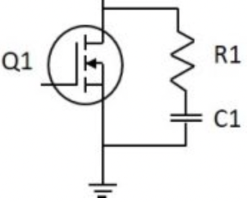
2. (2 points) Figure 1 shows a MOSFET with an RC circuit in parallel, which of the following answer best
describes the RC circuit?
A. Soft switching converter
B. Low pass filter
C. Snubber circuit
D. Resonant circuit
Figure 1: Image for multiple choice question 2

3. (2 points) Which switching technology will work best for high power, high voltage (greater than 6kV),
high current, low switching frequency applications?
A. IGBT
B. Thyristor
C. MOSFET
D. GTO
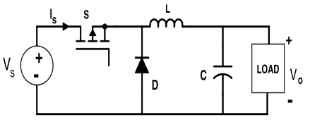
4. (2 points) The circuit shown in figure 2 can:
A. Step up the input voltage
B. Step down the input voltage
C. Step up or down the the input voltage
D. Increase the output power
Figure 2: Image for multiple choice question 4
5. (2 points) In continuous conduction mode, the switching frequency in a DC/DC converter influences
which following properties:
A. Input voltage
B. Inductor ripple magnitude
C. Component size
D. Efficiency of the converter
6. (2 points) What determines if a standard buck converter is synchronous rather than asynchronous?
A. The low side switch is controllable
B. The diode is fast recovery
C. The inductor current ripple stays positive
D. The converter can step up or down the output voltage
Page 2
7. (2 points) What is soft switching designed to avoid?
A. Rising edge resonance
B. Switching losses
C. Zero voltage crossing
D. All of the above
8. (2 points) What is the function of deadtime?
A. Ensure the high-side switch has an adequate Vgs
B. Increase system efficiency
C. Avoid shoot through current
D. Reduces switching frequency
9. (2 points) The main function of a boost converter is to:
A. Step up or down the input voltage
B. Step up the input voltage
C. Step down the voltage
D. Keep the converter in continuous conduction mode
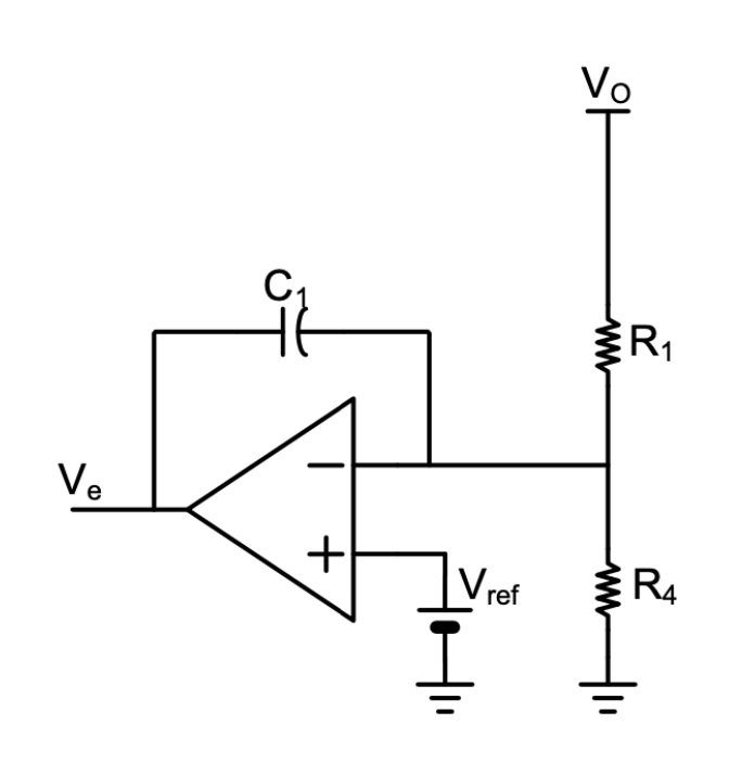
10. (2 points) What type of feedback controller is shown in figure
A. PD controller
B. PI controller
C. Type 2
D. Type 1
Figure 3: Image for multiple choice question 10
Page 3
DC/DC converter design
11. (30 points) You and your friends have planned to stay at a remote cabin in the woods to study for your
second EEEN313 test. The cabin does not have mains power, but has a solar installation which outputs
between 12V and 18V DC. There are three of you in the cabin, each with a laptop that needs to be
charged during the day, but not all laptops will necessarily be on at the same time. The laptops all run
off 20V, one is 45W, one 55W and the last 65W (you can assume resistive loads).
Design a converter that will stay in continuous conduction mode throughout the various charging loads
and can supply 20V to the laptops. Your switching frequency will be 30kHz and the output voltage
ripple should be no more than 5% (the output capacitor has an ESR of 0.2Ω)
Page 4
Space for additional working
Page 5
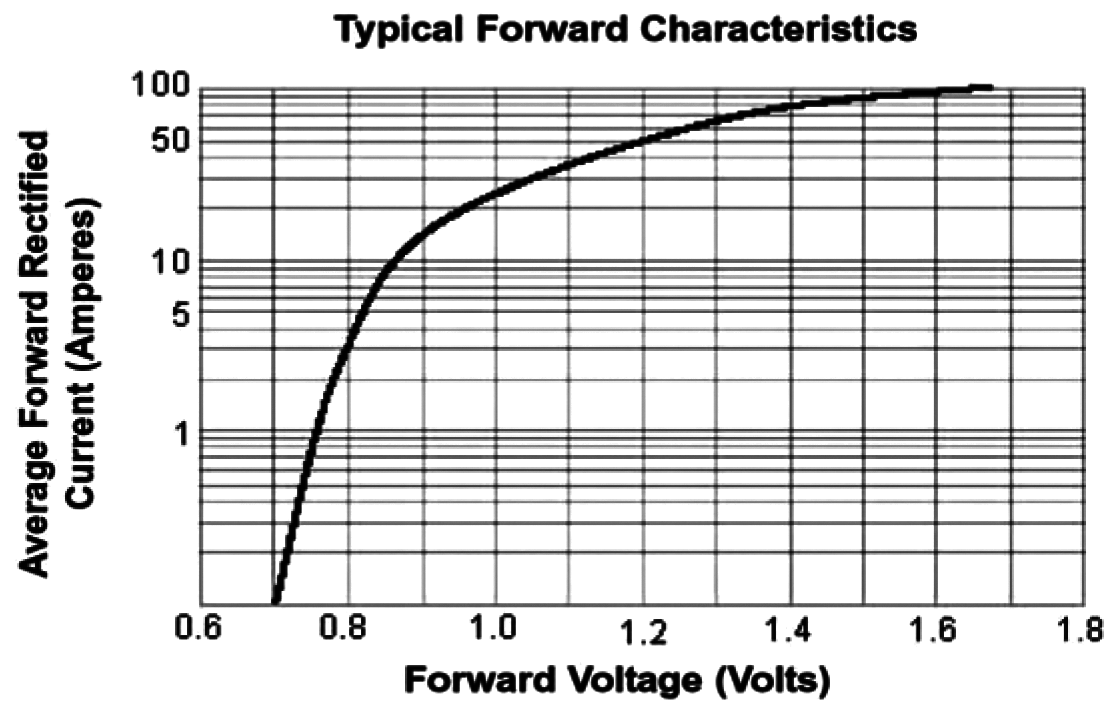
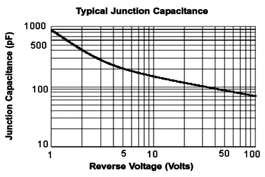
12. (20 points) Attached to this test is a datasheet for a MOSFET and for a fast recovery diode.
(a) (15 points) Calculate the losses in the switches of your laptop power supply converter.
(b) (5 points) What impact will these losses have on the duty cycle you give your converter? (discuss)
Page 6
Space for additional working
Page 7
13. (10 points) Calculate the ◦C/W required for heat sink to dissipate, in order to keep the MOSFET at
an appropriate temperature (you may also use case to sink from the datasheet and you can assume the
ambient temperature is 50◦C)
Page 8
Space for additional working
Page 9
Feedback
14. (20 points) A buck convert has a bode as shown in figure 4.
Bode Diagram
50
0
Magnitude (dB)
-50
0
-45
-90
Phase (deg) -135
-180
101
102
103
104
105
Frequency (rad/s)
Figure 4: Image for multiple choice question 14
(a) (10 points) Give the transfer function for a proportional integral (PI) controller that will ensure
the phase margin of the system remains unchanged. You do not need to plot the system but please
explain your answer.
Page 10
(b) (10 points) Assuming you are implementing an op-amp based PI controller, calculate values for
your capacitor and Ri. Your Rf value is 10kΩ
Page 11
Space for additional working
Page 12
Potentially helpful formulas:
Vo = D × Vin
Vo = D V
V
1−D
in
Vo =
1
1−D
in
Pcond = RDS(on) × D × I2
Psw = 1 × V
2
in × Io(tc,on + tc,of f )Fs
Pf = (1 − D)VF M × Io
Psw(diode) = Vd,neg( 1 × I
× F
2
RRM × trr )Fs
Ps = Cs × V 2
s
s
L = Vout(1−D)
L = D×Vin
L = Vin(Vout−Vin)
Fsw×∆IL
Fs×∆IL
Fs×∆IL×Vout
I2
×L
C
L(max)
o =
C
C
(V
o =
D×Io
∆I
o =
D×Iout
o +Vos )2 −V 2
L
F
o
Fs(Vo−( Io +
)ESR)
s ×∆Vout
1−D
2
∆I
Vout
Vout
L = 0.2 to 0.4 × Iout
∆IL = 0.2 to 0.4 × Iout
∆I
V
L = 0.2 to 0.4 × Iout
in
Vin
Θja = Θjc + Θcs + Θsa = Tj−Ta
Θ
Q
cs = ρ×t
A
Kp = Rf
K
s = −
1
R
i =
1
i
Ri×C
Rf ×C
C
s+ωb
(s) = C0
C
+ 1)
C
s
(s) = Co( s
ω
(s,type 1) =
1
b
sR1C
Page 13


 APT17F100B
APT17F100S
1000V, 17A, 0.78Ω Max, trr ≤245ns
N-Channel FREDFET
APT17F100B
APT17F100S
1000V, 17A, 0.78Ω Max, trr ≤245ns
N-Channel FREDFET
TO-247
Power MOS 8™ is a high speed, high voltage N-channel switch-mode power MOSFET.
D3PAK
This 'FREDFET' version has a drain-source (body) diode that has been optimized for
high reliability in ZVS phase shifted bridge and other circuits through reduced trr, soft
recovery, and high recovery dv/dt capability. Low gate charge, high gain, and a greatly
reduced ratio of Crss/Ciss result in excellent noise immunity and low switching loss. The
APT17F100B
APT17F100S
intrinsic gate resistance and capacitance of the poly-silicon gate structure help control
di/dt during switching, resulting in low EMI and reliable paralleling, even when switching
Single die FREDFET
at very high frequency.
FEATURES
TYPICAL APPLICATIONS
• Fast switching with low EMI
• ZVS phase shifted and other full bridge
• Low t
• Half bridge
rr for high reliability
• Ultra low C
• PFC and other boost converter
rss for improved noise immunity
• Low gate charge
• Buck converter
• Avalanche energy rated
• Single and two switch forward
• RoHS compliant
• Flyback
Absolute Maximum Ratings
Symbol
Parameter
Ratings
Unit
Continuous Drain Current @ T = 25°C
17
C
ID
Continuous Drain Current @ T = 100°C
C
11
A
IDM
Pulsed Drain Current 1
70
VGS
Gate-Source Voltage
±30
V
EAS
Single Pulse Avalanche Energy 2
1070
mJ
IAR
Avalanche Current, Repetitive or Non-Repetitive
9
A
Thermal and Mechanical Characteristics
Symbol
Characteristic
Min Typ Max
Unit
PD
Total Power Dissipation @ T = 25°C
625
W
C
R
Junction to Case Thermal Resistance
0.20
θJC
°C/W
R
Case to Sink Thermal Resistance, Flat, Greased Surface
0.11
θCS
T ,T
Operating and Storage Junction Temperature Range
-55
150
J
STG
°C
T
Soldering Temperature for 10 Seconds (1.6mm from case)
300
L
0.22
oz
1
WT
Package Weight
5.9
g
10
in·lbf
Torque
Mounting Torque ( TO-247 Package), 6-32 or M3 screw
1.1 N·m
Microsemi Website - http://www.microsemi.com
050-8159 Rev D 8-201
 Static Characteristics
TJ = 25°C unless otherwise specifi ed
APT17F100B_S
Symbol
Parameter
Test Conditions
Min Typ Max
Unit
Static Characteristics
TJ = 25°C unless otherwise specifi ed
APT17F100B_S
Symbol
Parameter
Test Conditions
Min Typ Max
Unit
VBR(DSS)
Drain-Source Breakdown Voltage
V
= 0V, I = 250μA
1000
V
GS
D
∆V
/∆T
BR(DSS)
J
Breakdown Voltage Temperature Coeffi cient
Reference to 25°C, I = 250μA
1.15
V/°C
D
RDS(on)
Drain-Source On Resistance 3
V
= 10V, I = 9A
0.67 0.78
Ω
GS
D
VGS(th)
Gate-Source Threshold Voltage
2.5
4
5
V
V
= V , I = 1mA
∆V
/∆T
GS
DS
D
GS(th)
J
Threshold Voltage Temperature Coeffi cient
-10
mV/°C
V
= 1000V
T = 25°C
250
DS
J
I
Zero Gate Voltage Drain Current
μA
DSS
V
= 0V
T = 125°C
1000
GS
J
I
Gate-Source Leakage Current
V
= ±30V
GSS
±100
nA
GS
Dynamic Characteristics
TJ = 25°C unless otherwise specifi ed
Symbol
Parameter
Test Conditions
Min Typ Max
Unit
g
V
fs
Forward Transconductance
= 50V, I = 9A
DS
D
19
S
Ciss
Input Capacitance
4845
V
= 0V, V = 25V
C
GS
DS
rss
Reverse Transfer Capacitance
65
f = 1MHz
Coss
Output Capacitance
405
pF
C
4
Effective Output Capacitance, Charge Related
165
o(cr)
V
= 0V, V = 0V to 667V
GS
DS
C
5
Effective Output Capacitance, Energy Related
o(er)
85
Q
Total Gate Charge
g
150
V
= 0 to 10V, I = 9A,
Q
GS
D
gs
Gate-Source Charge
26
nC
V
= 500V
DS
Qgd
Gate-Drain Charge
70
t
Resistive Switching
d(on)
Turn-On Delay Time
29
t
Current Rise Time
V
= 667V, I = 9A
r
DD
D
31
ns
t
Turn-Off Delay Time
R = 4.7Ω 6 , V
= 15V
d(off)
G
GG
105
t
Current Fall Time
f
28
Source-Drain Diode Characteristics
Symbol
Parameter
Test Conditions
Min Typ Max
Unit
Continuous Source Current
I
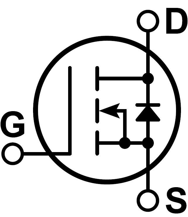
MOSFET symbol
S
17
(Body Diode)
showing the
integral reverse p-n
A
Pulsed Source Current
junction diode
ISM
65
(body diode)
(Body Diode) 1
V
I
= 9A, T = 25°C, V = 0V
SD
Diode Forward Voltage
SD
J
GS
1.2
V
T = 25°C
J
215 245
trr
Reverse Recovery Time
ns
T = 125°C
J
385 465
I
= 9A 3
T = 25°C
SD
J
1.02
Qrr
Reverse Recovery Charge
μC
di
/dt = 100A/μs
T = 125°C
SD
J
2.57
V
= 100V
T = 25°C
DD
J
9.03
Irrm
Reverse Recovery Current
A
T = 125°C
J
12.83
I
≤ 9A, di/dt ≤1000A/μs, V
= 400V,
SD
DD
dv/dt
Peak Recovery dv/dt
25
V/ns
T = 125°C
J
1 Repetitive Rating: Pulse width and case temperature limited by maximum junction temperature.
2 Starting at T = 25°C, L = 26.42mH, R = 25Ω, I
= 9A.
J
G
AS
3 Pulse test: Pulse Width < 380μs, duty cycle < 2%.
1
4 C
is defi ned as a fi xed capacitance with the same stored charge as C
with V
= 67% of V
.
o(cr)
OSS
DS
(BR)DSS
5 C
is defi ned as a fi xed capacitance with the same stored energy as C
with V
= 67% of V
. To calculate C
for any value of
o(er)
OSS
DS
(BR)DSS
o(er)
V
less than V
use this equation: C
= -1.41E-8/V ^2 + 2.48E-9/V
+ 4.81E-11.
DS
(BR)DSS,
o(er)
DS
DS
6 R is external gate resistance, not including internal gate resistance or gate driver impedance. (MIC4452)
G
Microsemi reserves the right to change, without notice, the specifi cations and information contained herein.
050-8159 Rev D 8-201
 Ultra Fast Rectifiers
Features
Ultra Fast Rectifiers
Features
• Glass passivated chip junctions
• Low reverse leakage current
• Fast switching for high efficiency
• 150°C operating junction temperature
• Low stored charge majority carrier conduction
• Low forward voltage, high current capability
• Plastic material used carries Underwriters Laboratory
• Flammability classification 94V-0
Specifications
Reverse Voltage : 200 Volts
Forward Current : 30 Amperes
Maximum Ratings
Characteristic
Symbol
Values
Units
Peak Repetitive Reverse Voltage
Vrrm
Working Peak Reverse Voltage
Vrwm
200
DC Blocking Voltage
V
V
r
RMS Reverse Voltage
Vr(rms)
140
Average Rectifier Forward Current
15
I
Total Device (Rated V
f(av)
r), Tc = 125°C
30
Peak Repetitive Forward Current
Ifm
30
A
(Rate Vr, Square Wave, 20kHz)
Non-Repetitive Peak Surge Current (Surge applied
at rate load conditions half-ware, single phase, 60Hz)
Ifsm
300
Operating and Storage Junction Temperature Range
Tj, Tstg
-65 to +150
°C
Electrical Characteristics
Characteristic
Symbol
Values
Units
Maximum Instantaneous Forward Voltage
(If = 15 Amperes Tc = 25°C)
vf
0.975
V
(If = 15 Amperes Tc = 125°C)
0.88
Maximum Instantaneous Reverse Current
(Rated DC Voltage, Tc = 25°C)
Ir
10
μA
(Rated DC Voltage, Tc = 125°C)
500
Reverse Recovery Time
t
(If = 0.5A, Ir = 1 lrr = 0.25A)
rr
35
ns
Typical Junction Capacitance
C
(Reverse Voltage of 4 volts and f = 1MHz)
p
250
pF
Newark.com/multicomp-pro
Farnell.com/multicomp-pro
Element14.com/multicomp-pro
Page <1>
03/02/20 V1.0


 Ultra Fast Rectifiers
Newark.com/multicomp-pro
Farnell.com/multicomp-pro
Element14.com/multicomp-pro
Page <2>
03/02/20 V1.0
Space for additional working
Page 18
Space for additional working
Page 19
Space for additional working
Page 20
Space for additional working
Page 21
EEEN313
Test 2
Total marks: 70 (Contribution: 20)
Instructions:
Do your calculation as needed and then put your final answers as well any discussion or
plots in the spaces required.
Submit this document with a filename:
EEEN313_Test2_”your surname”-“your initial” on Blackboard. Once you have started the
test, it must be completed in the 2 hour time allocated.
Name: ……………………………………………………………………………………………..
Student Number:……………………………………………………………………………….
Q1. In a single-phase diode rectifier bridge, Is = 10A(rms), Is1 = 8A(rms), and DPF = 0.85.
Calculate Idistortion, %
THD, and PF.
Answer
(10)
Q2. Calculate the percentage
harmonic distortion of individual component and total THD for
an output signal having a fundamental amplitude of 5 V, second harmonic amplitude of 0.5V and
a third and fourth harmonic components of 0.3 and 0.2.
Answer
(10)
 Q3.
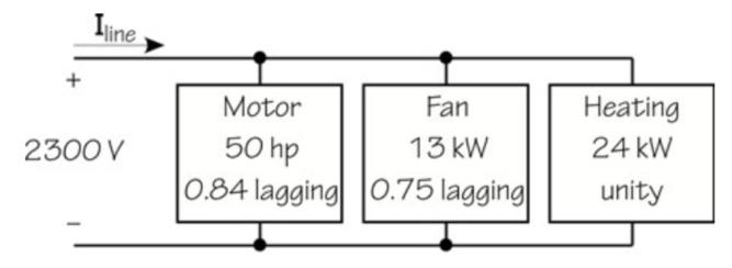
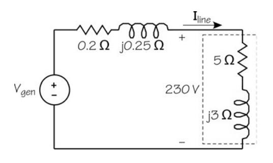
Q3. Find Real, Reactive and Apparent power for following load configuration.
Answer:
(15)
 Q4.
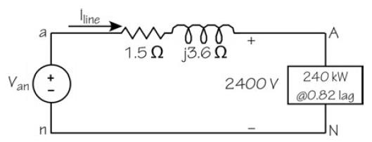
Q4. A 4,160-V, 50-Hz, 3∅ system supplies a 720-kW load at 0.82 lagging power factor
through lines with a line impedance of 1.5 + j3.6 Ω/∅. (∅ is often written for “phase.”) Find the
line current, the percent efficiency, the percent voltage regulation, and the generator power
factor, and generator voltage.
Answer:
(20)
 Q6.
Q6. For the following circuit, find P, Q and the power factor.
Answer:
(15)
EEEN313 Test 1
Time Allowed: 50 minutes
Instructions: Answer ALL questions on the paper provided and show working where
possible. There are 12 questions, of which 10 are multiple choice.
It is essential all answers given are your own, you must not work with anyone else
during the test
For the multiple choice questions, circle the letter that corresponds to the answers that
you believe are correct (there can be more than one correct answer for each question)
Potentially useful formulas, datasheets and additional working space can be found at
the end of this test.
Student name:
Student number:
Multiple Choice (20 points)
1. (2 points) Which of the following statements best describes the term ‘Mf ’ ?
A. Magnitude of the switching frequency (Fs)
B. The ratio of frequency, between the carrier frequency (Fc) and signal frequency (Fs) → Fc )
Fs
C. Switching frequency of the phase locked loop (PLL) voltage controlled oscillator (VCO)
D. The ratio of proportional gain (Kp) to integral gain (Ki) in a PI system
2. (2 points) Which of the following answers best describes discontinuous conduction mode?
A. The inductor current ripple falls to zero
B. The inductor voltage ripple goes negative
C. The output current ripple falls to zero
D. The inductor current ripple stays positive
3. (2 points) Which of the following statements are true?
A. The SEPIC converter has an inverting output, and benefits from a coupled inductor
B. The buck-boost converter has an inverting output, and benefits from a coupled inductor
C. The C´
uk converter has a higher component count than the SEPIC converter
D. The SEPIC converter has a non-inverting output and a higher component count than the
buck-boost converter
E. None of the above
4. (2 points) The circuit shown in figure 1 can:
A. Step up the input voltage
B. Step down the input voltage
C. Step up or down the the input voltage
D. Increase the output power
Figure 1: Image for multiple choice question 4
5. (2 points) In continuous conduction mode, the switching frequency in a DC/DC converter influences
which following properties:
A. Input voltage
B. Inductor ripple magnitude
C. Component size
D. Efficiency of the converter
6. (2 points) What determines if a standard buck converter is synchronous rather than asynchronous?
A. The low side switch is controllable
B. The diode is fast recovery
C. The inductor current ripple stays positive
D. The converter can step up or down the output voltage
Page 2
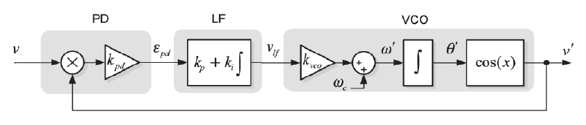
7. (2 points) Figure 2 displays a block diagram of what type of circuit?
A. Proportional derivative
B. Triangle wave generator
C. Phase locked loop
D. Proportional integral
Figure 2: Image for multiple choice question 7
8. (2 points) What is the function of deadtime?
A. Ensure the high-side switch has an adequate Vgs
B. Increase system efficiency
C. Avoid shoot through current
D. Reduces switching frequency
9. (2 points) The main function of a boost converter is to:
A. Step up or down the input voltage
B. Step up the input voltage
C. Step down the voltage
D. Keep the converter in continuous conduction mode
10. (2 points) What type of feedback controller is shown in figure 3?
A. PD controller
B. PI controller
C. Type 2
D. Type 1
Page 3

Figure 3: Image for multiple choice question 10
DC/DC converter design (50 points)
11. (30 points) You are building a 100W 500V power supply for a large DC motor you are driving. You have
230V RMS Mains power (50Hz) which you first must rectify and smooth to within a 1% voltage ripple.
Once you have rectified the AC to DC voltage, you must design a DC/DC converter to achieve your 500V
output. Your converter will have a switching frequency of 50kHz, require an inductor current ripple of
20% and an output voltage ripple of 5% . If you cannot calculate the rectifier, give an approximate input
voltage to your converter. Ensure that you sketch a picture of your circuit from Vin
to V
AC
outDC
Page 4
Space for additional working
Page 5
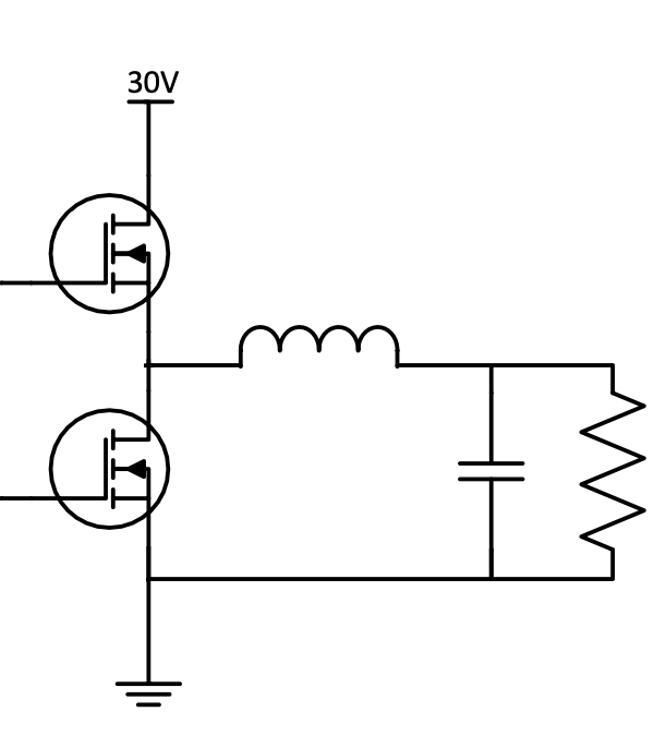
12. (20 points) You have been asked to help with the design of a heat sink for the buck converter picture
in figure 4. It has the following characteristics:
• Input power of 200W
• Input voltage of 50V
• Output voltage of 25V
• Switching frequency of 100kHz
Figure 4: Image for question 12
Attached to this test is a datasheet for a MOSFET and for a fast recovery diode that will be used in the
Buck converter (fig. 4)
(a) (15 points) Calculate the losses contributed by the switches of your converter.
(b) (5 points) What impact will these losses have on the duty cycle you give your converter? (briefly
discuss)
Page 6
Space for additional working
Page 7

Potentially helpful formulas:
Vo = D × Vin
Vo = D V
V
1−D
in
Vo =
1
1−D
in
Pcond = RDS(on) × D × I2
Psw = 1 × V
2
in × I (tc,on + tc,of f )Fs
Pf = (1 − D)VF M × I
Psw(diode) = Vd,neg( 1 × I
× F
2
RRM × trr )Fs
Ps = Cs × V 2
s
s
L = Vout(1−D)
L = D×Vin
L = Vin(Vout−Vin)
Fsw×∆IL
Fs×∆IL
Fs×∆IL×Vout
I2
×L
C
L(max)
o =
C
C
(V
o =
D×Io
∆I
o =
D×Iout
o +Vos )2 −V 2
L
F
o
Fs(Vo−( Io +
)ESR)
s ×∆Vout
1−D
2
∆I
Vout
L = 0.2 to 0.4 × Iout
∆IL = 0.2 to 0.4 × Iout
∆I
V
L = 0.2 to 0.4 × (Iin + Iout)
in
√
VDC = 2Vmax
V
2 × V
π
max =
RM S
V(ripple) = IDC
2f C
Kp = Rf
K
s = −
1
R
i =
1
i
Ri×C
Rf ×C
C
s+ωb
(s) = C0
C
+ 1)
C
s
(s) = Co( s
ω
(s,type 1) =
1
b
sR1C
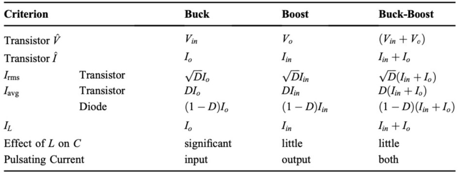
Figure 5: Switch stresses
Page 8


 APT17F100B
APT17F100S
1000V, 17A, 0.78Ω Max, trr ≤245ns
N-Channel FREDFET
APT17F100B
APT17F100S
1000V, 17A, 0.78Ω Max, trr ≤245ns
N-Channel FREDFET
TO-247
Power MOS 8™ is a high speed, high voltage N-channel switch-mode power MOSFET.
D3PAK
This 'FREDFET' version has a drain-source (body) diode that has been optimized for
high reliability in ZVS phase shifted bridge and other circuits through reduced trr, soft
recovery, and high recovery dv/dt capability. Low gate charge, high gain, and a greatly
reduced ratio of Crss/Ciss result in excellent noise immunity and low switching loss. The
APT17F100B
APT17F100S
intrinsic gate resistance and capacitance of the poly-silicon gate structure help control
di/dt during switching, resulting in low EMI and reliable paralleling, even when switching
Single die FREDFET
at very high frequency.
FEATURES
TYPICAL APPLICATIONS
• Fast switching with low EMI
• ZVS phase shifted and other full bridge
• Low t
• Half bridge
rr for high reliability
• Ultra low C
• PFC and other boost converter
rss for improved noise immunity
• Low gate charge
• Buck converter
• Avalanche energy rated
• Single and two switch forward
• RoHS compliant
• Flyback
Absolute Maximum Ratings
Symbol
Parameter
Ratings
Unit
Continuous Drain Current @ T = 25°C
17
C
ID
Continuous Drain Current @ T = 100°C
C
11
A
IDM
Pulsed Drain Current 1
70
VGS
Gate-Source Voltage
±30
V
EAS
Single Pulse Avalanche Energy 2
1070
mJ
IAR
Avalanche Current, Repetitive or Non-Repetitive
9
A
Thermal and Mechanical Characteristics
Symbol
Characteristic
Min Typ Max
Unit
PD
Total Power Dissipation @ T = 25°C
625
W
C
R
Junction to Case Thermal Resistance
0.20
θJC
°C/W
R
Case to Sink Thermal Resistance, Flat, Greased Surface
0.11
θCS
T ,T
Operating and Storage Junction Temperature Range
-55
150
J
STG
°C
T
Soldering Temperature for 10 Seconds (1.6mm from case)
300
L
0.22
oz
1
WT
Package Weight
5.9
g
10
in·lbf
Torque
Mounting Torque ( TO-247 Package), 6-32 or M3 screw
1.1 N·m
Microsemi Website - http://www.microsemi.com
050-8159 Rev D 8-201
 Static Characteristics
TJ = 25°C unless otherwise specifi ed
APT17F100B_S
Symbol
Parameter
Test Conditions
Min Typ Max
Unit
Static Characteristics
TJ = 25°C unless otherwise specifi ed
APT17F100B_S
Symbol
Parameter
Test Conditions
Min Typ Max
Unit
VBR(DSS)
Drain-Source Breakdown Voltage
V
= 0V, I = 250μA
1000
V
GS
D
∆V
/∆T
BR(DSS)
J
Breakdown Voltage Temperature Coeffi cient
Reference to 25°C, I = 250μA
1.15
V/°C
D
RDS(on)
Drain-Source On Resistance 3
V
= 10V, I = 9A
0.67 0.78
Ω
GS
D
VGS(th)
Gate-Source Threshold Voltage
2.5
4
5
V
V
= V , I = 1mA
∆V
/∆T
GS
DS
D
GS(th)
J
Threshold Voltage Temperature Coeffi cient
-10
mV/°C
V
= 1000V
T = 25°C
250
DS
J
I
Zero Gate Voltage Drain Current
μA
DSS
V
= 0V
T = 125°C
1000
GS
J
I
Gate-Source Leakage Current
V
= ±30V
GSS
±100
nA
GS
Dynamic Characteristics
TJ = 25°C unless otherwise specifi ed
Symbol
Parameter
Test Conditions
Min Typ Max
Unit
g
V
fs
Forward Transconductance
= 50V, I = 9A
DS
D
19
S
Ciss
Input Capacitance
4845
V
= 0V, V = 25V
C
GS
DS
rss
Reverse Transfer Capacitance
65
f = 1MHz
Coss
Output Capacitance
405
pF
C
4
Effective Output Capacitance, Charge Related
165
o(cr)
V
= 0V, V = 0V to 667V
GS
DS
C
5
Effective Output Capacitance, Energy Related
o(er)
85
Q
Total Gate Charge
g
150
V
= 0 to 10V, I = 9A,
Q
GS
D
gs
Gate-Source Charge
26
nC
V
= 500V
DS
Qgd
Gate-Drain Charge
70
t
Resistive Switching
d(on)
Turn-On Delay Time
29
t
Current Rise Time
V
= 667V, I = 9A
r
DD
D
31
ns
t
Turn-Off Delay Time
R = 4.7Ω 6 , V
= 15V
d(off)
G
GG
105
t
Current Fall Time
f
28
Source-Drain Diode Characteristics
Symbol
Parameter
Test Conditions
Min Typ Max
Unit
Continuous Source Current
I
MOSFET symbol
S
17
(Body Diode)
showing the
integral reverse p-n
A
Pulsed Source Current
junction diode
ISM
65
(body diode)
(Body Diode) 1
V
I
= 9A, T = 25°C, V = 0V
SD
Diode Forward Voltage
SD
J
GS
1.2
V
T = 25°C
J
215 245
trr
Reverse Recovery Time
ns
T = 125°C
J
385 465
I
= 9A 3
T = 25°C
SD
J
1.02
Qrr
Reverse Recovery Charge
μC
di
/dt = 100A/μs
T = 125°C
SD
J
2.57
V
= 100V
T = 25°C
DD
J
9.03
Irrm
Reverse Recovery Current
A
T = 125°C
J
12.83
I
≤ 9A, di/dt ≤1000A/μs, V
= 400V,
SD
DD
dv/dt
Peak Recovery dv/dt
25
V/ns
T = 125°C
J
1 Repetitive Rating: Pulse width and case temperature limited by maximum junction temperature.
2 Starting at T = 25°C, L = 26.42mH, R = 25Ω, I
= 9A.
J
G
AS
3 Pulse test: Pulse Width < 380μs, duty cycle < 2%.
1
4 C
is defi ned as a fi xed capacitance with the same stored charge as C
with V
= 67% of V
.
o(cr)
OSS
DS
(BR)DSS
5 C
is defi ned as a fi xed capacitance with the same stored energy as C
with V
= 67% of V
. To calculate C
for any value of
o(er)
OSS
DS
(BR)DSS
o(er)
V
less than V
use this equation: C
= -1.41E-8/V ^2 + 2.48E-9/V
+ 4.81E-11.
DS
(BR)DSS,
o(er)
DS
DS
6 R is external gate resistance, not including internal gate resistance or gate driver impedance. (MIC4452)
G
Microsemi reserves the right to change, without notice, the specifi cations and information contained herein.
050-8159 Rev D 8-201
 Ultra Fast Rectifiers
Features
Ultra Fast Rectifiers
Features
• Glass passivated chip junctions
• Low reverse leakage current
• Fast switching for high efficiency
• 150°C operating junction temperature
• Low stored charge majority carrier conduction
• Low forward voltage, high current capability
• Plastic material used carries Underwriters Laboratory
• Flammability classification 94V-0
Specifications
Reverse Voltage : 200 Volts
Forward Current : 30 Amperes
Maximum Ratings
Characteristic
Symbol
Values
Units
Peak Repetitive Reverse Voltage
Vrrm
Working Peak Reverse Voltage
Vrwm
200
DC Blocking Voltage
V
V
r
RMS Reverse Voltage
Vr(rms)
140
Average Rectifier Forward Current
15
I
Total Device (Rated V
f(av)
r), Tc = 125°C
30
Peak Repetitive Forward Current
Ifm
30
A
(Rate Vr, Square Wave, 20kHz)
Non-Repetitive Peak Surge Current (Surge applied
at rate load conditions half-ware, single phase, 60Hz)
Ifsm
300
Operating and Storage Junction Temperature Range
Tj, Tstg
-65 to +150
°C
Electrical Characteristics
Characteristic
Symbol
Values
Units
Maximum Instantaneous Forward Voltage
(If = 15 Amperes Tc = 25°C)
vf
0.975
V
(If = 15 Amperes Tc = 125°C)
0.88
Maximum Instantaneous Reverse Current
(Rated DC Voltage, Tc = 25°C)
Ir
10
μA
(Rated DC Voltage, Tc = 125°C)
500
Reverse Recovery Time
t
(If = 0.5A, Ir = 1 lrr = 0.25A)
rr
35
ns
Typical Junction Capacitance
C
(Reverse Voltage of 4 volts and f = 1MHz)
p
250
pF
Newark.com/multicomp-pro
Farnell.com/multicomp-pro
Element14.com/multicomp-pro
Page <1>
03/02/20 V1.0


 Ultra Fast Rectifiers
Newark.com/multicomp-pro
Farnell.com/multicomp-pro
Element14.com/multicomp-pro
Page <2>
03/02/20 V1.0
Space for additional working
Page 13
Space for additional working
Page 14
EEEN313
Test 2
Total marks: 70 (Contribution: 20)
Instructions:
Do your calculation as needed and then put your final answers as well any discussion or
plots in the spaces required.
Submit this document with a filename:
EEEN313_Test2_”your surname”-“your initial” on Blackboard. Once you have started the
test, it must be completed in the 2 hour time allocated.
Name: ……………………………………………………………………………………………..
Student Number:……………………………………………………………………………….
Q1. In a single-phase diode rectifier bridge, Is = 10A(rms), Is1 = 8A(rms), and DPF = 0.85.
Calculate Idistortion, %
THD, and PF.
Answer
(10)
Q2. Calculate the percentage
harmonic distortion of individual component and total THD for
an output signal having a fundamental amplitude of 5 V, second harmonic amplitude of 0.5V and
a third and fourth harmonic components of 0.3 and 0.2.
Answer
(10)
 Q3.
Q3. Find Real, Reactive and Apparent power for following load configuration.
Answer:
(15)
 Q4.
Q4. A 4,160-V, 50-Hz, 3∅ system supplies a 720-kW load at 0.82 lagging power factor
through lines with a line impedance of 1.5 + j3.6 Ω/∅. (∅ is often written for “phase.”) Find the
line current, the percent efficiency, the percent voltage regulation, and the generator power
factor, and generator voltage.
Answer:
(20)
 Q6.
Q6. For the following circuit, find P, Q and the power factor.
Answer:
(15)


EEEN313 Test 1
Time Allowed: 50 minutes
Instructions: Answer ALL questions on the paper provided and show working where
possible. There is 1 question with parts a) through g) for EEEN313 students, and an
additional question (part a) through c)) for RESE413 students
It is essential all answers given are your own, you must not work with anyone else
during the test
Potentially useful formulas and additional working space can be found at the end of
this test.
Student name:
Student number:
DC/DC converter design (100 points)
1. (100 points) You have been asked to design a power supply for a 19V, 80W laptop (Converter Vout = 19V
and Pout = 80W ), that can operate in various vehicles (Cars (12V), trucks and caravans (24V). It must
have an inductor current ripple of no greater than 20%, and an output voltage ripple of 5%. The PWM
you are working with has a frequency of 80kHz. Please:
(a) (6 points) Identify (a, b or c) and label (buck, boost or buck-boost) the appropriate converter for
this task, from the image below.
a)
b)
c)
(b) (34 points) Size the converter inductor and output capacitor
(c) (10 points) There are a number of MOSFETs and diodes available for this, relevant information
from the datasheets are given in table 1 (MOSFETs) and 2 (diodes). Select the most appropriate
MOSFET and diode for the job (motivate your answer).
Selected MOSFET:
Selected Diode:
Page 2
Table 1: Available MOSFETs
Identifier
Max voltage
Max current
Rise time
Fall time
RDS(on)
M1
40V
20A
88nS
67nS
6.5mΩ
M2
65V
18A
30nS
26nS
37mΩ
M3
100V
12A
20nS
16nS
10mΩ
M4
36V
20A
38nS
20nS
22mΩ
M5
80V
22A
96nS
58nS
40mΩ
M6
70V
17A
28nS
25nS
80mΩ
Table 2: Available diodes
Identifier
Max voltage
Max current
Forward voltage drop
D1
100V
22A
1.15V
D2
20V
20A
0.42V
D3
65V
17A
0.78V
D4
80V
10A
0.36V
D5
70V
25A
1.2V
(d) (20 points) Calculate the losses in the switches (note: the diodes are fast recovery, so switching
losses do not have to be calculated for the diode.)
Page 3
(e) (10 points) What effect would the losses have on the output voltage and how might you mitigate
these effects? (think back to what you saw in the lab)
(f) (10 points) It is assumed the converter is asynchronous. If the converter is changed to synchronous,
would the efficiency increase?
(g) (10 points) Briefly describe what is meant by discontinuous conduction mode, and calculate the
lowest switching frequency you can run your designed converter at before it enters discontinuous
conduction mode.
***** End of EEEN313 Test *****
Page 4
RESE413 only (20 points)
2. (20 points) Briefly describe the following:
(a) (8 points) What is the function of a gate driver?
(b) (5 points) What is the maximum inductor current ripple a buck converter can have before it enters
discontinuous conduction mode?
(c) (7 points) What is the voltage drop across a boost converter’s inductor during the “on” and “off”
switching cycle?
Page 5
Potentially helpful formulas (given in no particular order, as in, the columns don’t mean
anything):
Vo = D × Vin
Vo = D V
× V
1−D
in
Psw = 12
in × I (tc,on + tc,of f )Fs
Pcond = RDS(on) × D × I2
Vo =
1
V
1−D
in
Pf = (1 − D)VF M × I
P
Vout
sw(diode) = Vd,neg ( 1 × I
P
2
RRM × trr )Fs
∆IL = 0.2 to 0.4 × Iout V
sw(diode) = Qrr Vd,neg Fs
in
v
∆t
L = L di
i
L = v
dt
C = C dv
dt
L ∆i
C = i ∆t
C
∆I
∆v
L = 0.2 to 0.4 × Iout
∆IL = 0.2 to 0.4 × (Iin + Iout)
√
VDC = 2Vmax
V
2 × V
π
max =
RM S
V(ripple) = IDC
2f C
Kp = Rf
K
s = −
1
R
i =
1
i
Ri×C
Rf ×C
C
s+ωb
(s) = C0
C
+ 1)
C
s
(s) = Co( s
ω
(s,type 1) =
1
b
sR1C
Figure 1: Switch stresses
Page 6
Space for additional working
Page 7
Space for additional working
Page 8
EEEN313/RESE413 Test 2
Time Allowed: 120 minutes (for EEEN313 and RESE413)
Instructions: Answer ALL questions on the paper provided and show working where
possible. There are 4 questions for EEEN313 students, and an additional question for
RESE413 students
For multi-choice questions, circle the letter of the appropriate answer
It is essential all answers given are your own, you must not work with anyone else
during the test
Potentially useful formulas and additional working space can be found at the end of
this test.
Student name:
Student number:
General knowledge (20 points)
1. (20 points) The following question is a mix of multi-choice and short answers:
(a) (2 points) In an AC system, which of the following statements best describes the behavior through
an inductive load:
A. The voltage and current are in phase
B. The current lags the voltage
C. The current leads the voltage
D. The voltage lags the current
(b) (2 points) If you were asked to improve the efficiency of a full wave diode rectifier, which of the
following would you implement?
A. Reduce the frequency
B. Reduce input voltage
C. MOSFET synchronous rectifier
D. Half wave rectifier
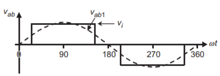
(c) (2 points) Shown in figure 1 is the switching/output wave of a square wave inverter. Describe the
advantages and disadvantages of this switching scheme (compared to PWM).
Figure 1: Inverter switching wave
(d) (2 points) A full wave diode rectifier, with 0.7V drop across each diode, is connected to a large
smoothing capacitor (as shown in figure 2). If the maximum output voltage is 36V, what is the
input RMS voltage? (show working)
(e) (2 points) Briefly describe the problems associated with a diode rectifier connected to a large
smoothing capacitor (shown in figure 2).
Page 2
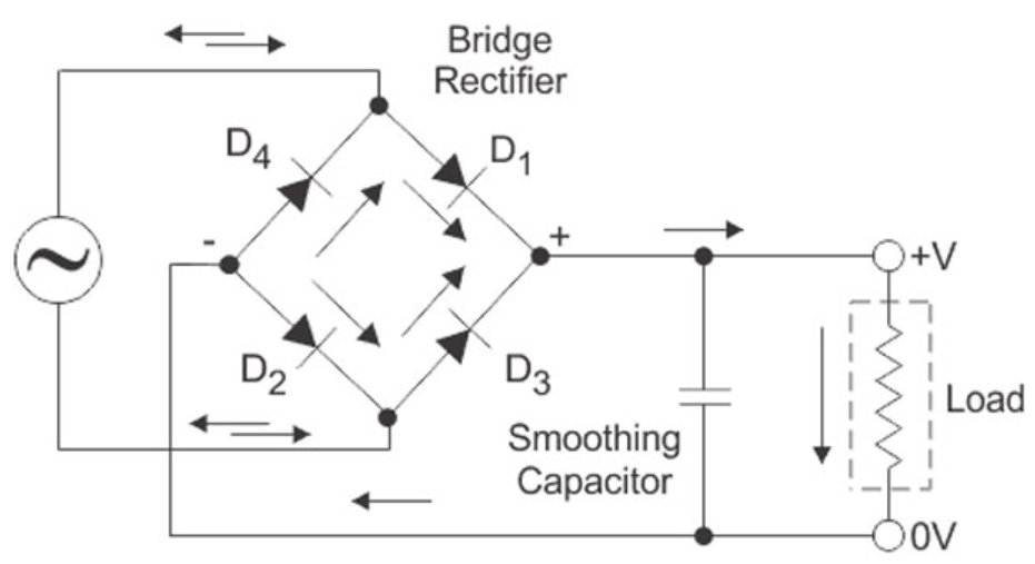
Figure 2: Full wave diode rectifier
(f) (4 points) Sketch a full wave rectifier with a power factor correction circuit connected
DC/AC conversion (20 points)
2. (25 points) You need to design a full bridge inverter, driven by a high frequency PWM, that outputs
AC at 150Hz with a voltage of 200V RMS. It will drive a load of 300W
(a) (5 points) Sketch the circuit connected to a DC supply
Page 3
(b) (5 points) What DC voltage do you need on the input of the full bridge, assuming a maximum duty
cycle of 90%
(c) (5 points) Select a switching frequency for the PWM that minimizes switching losses, passes the
150Hz and minimizes harmonics. Explain your answer.
(d) (10 points) Design an output LC filter for your inverter.
Page 4
Three Phase Induction Motor Modelling (40 points)
3. (40 points) Each phase of a three-phase induction motor can be described by an equivalent circuit model
as shown in Fig. 3 below.
I
R
1
1
X1
I'
R'
2
2
X'2
+
I
+
p
V1
E2
Rc
Xm
Rshaft
Figure 3: Induction motor equivalent circuit.
A 400 V, three-phase, 15 kW, 50 Hz, 8-pole induction motor has the following equivalent circuit model
′
′
parameters: R1 = 0.0162 Ω, X1 = 0.9903 Ω, R = 0.1587 Ω, X = 3.8174 Ω, X
2
2
m = 45.4817 Ω, and
Rc = 86.9641 Ω. Its full-load speed is 732 RPM.
Note: You can use the junction to split this problem into multiple stages and make the calculations
easier.
Use the model in Fig 3 to calculate the following:
(a) (2 points) The percentage slip.
(b) (2 points) The output shaft resistance Rshaft in Ohms.
(c) (2 points) The angular velocity in rad.s−1.
Page 5
(d) (2 points) The output torque in N.m.
(e) (2 points) The output Power per phase in kW.
′
(f) (2 points) The polar form of the current I in A.
2
(g) (4 points) The polar form of the voltage E2 in V.
(h) (6 points) The cartesian form of the current Ip in A.
Page 6
(i) (2 points) The cartesian form of the input current I1 in A.
(j) (6 points) The cartesian form of the input voltage V1 in V.
(k) (4 points) The input power Factor.
(l) (2 points) The input power per phase in kW.
(m) (2 points) The total input power in kW.
Page 7
(n) (2 points) The percentage motor efficiency.
Page 8
Three Phase Induction Motor Performance (15 points)
4. (15 points) The graph in Figure 4 below shows a torque versus speed curve for an 8 pole three phase
induction motor. The rated torque is given as 189.5 N.m at 2.4% slip.
250
200
150
100
50
Mechanical Torque (N.m)
0500 550 600 650 700 750 800
Motor Speed (RPM)
Figure 4: The torque-speed curve of a three-phase induction motor.
(a) (6 points) As the slip increases to 10%, what happens to the torque and motor speed?
Page 9
(b) (4 points) Approximately what is the breakdown torque and what RPM does it occur?
(c) (5 points) If you could no-longer purchase this motor, would you prefer to use a replacement motor
at 105% or 95% of rated load. Why would you choose this motor?
Note: you can assume that both motors can be functionally used in the system.
***** End of EEEN313 Test *****
Page 10
RESE413 only (20 points)
5. (20 points) In question 1f, you were asked to sketch a rectifier with PFC. Assuming an input AC voltage
of 300V RMS, a switching frequency of 20kHz, output power of 1kW and an output DC voltage of
500V :
(a) (6 points) What duty cycle range will your PFC operate at?
(b) (4 points) Sketch the expected voltage out of the rectifier (before the PFC smooths it) and the
control signal for the PWM of the PFC
(c) (10 points) Calculate an inductor value that will ensure a current ripple of 30%.
Page 11
-
Page 12
Potentially helpful formulas (given in no particular order, as in, the columns don’t mean
anything):
V(t) = Vmaxcos(ωt + δ)
V= Vmax
√
i
2
R(t) = IRmaxcos(ωt + δ)A
iL(t) = ILmaxcos(ωt + δ − 90)A
iC(t) = ICmaxcos(ωt + δ + 90)A
V IR{1 + cos[2(ωt + δ)]}
p
V I
(t) = V IR{1 + cos[2(ωt + δ]}
Lsin[2(ωt + δ)]
−V ICsin[2(ωt + δ)]
+V IX sin[2(ωt + δ)]
p
cos(δ − β)
S =
P 2 + Q2
IO = VO = 2Vm
R
πR
i
VO
C = C dv
=
1
D = 1 − Vmaxsin(ωt)
dt
Vin
1−D
VO
P = Vt E
(E
X
g sin(δ)
Q = Vt
g cos(δ) − Vt)
VL = L di
g
Xg
dt
Ma = vr
M
S = EgVt(jcos(δ)+sin(δ))−jV 2
t
v
f = fc
c
fr
Xg
∆imax = VDC×T
L =
VDC
F
4×L
4×∆i
c = Fsw
max Fsw
10
q
F
Linv+Lgrid
c =
1
√
fres = 1
fres ≈ fsw
2π
LC
2π
C×Linv×Lgrid
6
√
Rshaft = R2.(1−s)
r =
a2 + b2
θ = arctan b
s
a
RT = RP1.RP2
a = r. cos θ
b = r. sin θ
RP1+RP2
s = ns−n
n
.f
n
s = 120
e
Tout = Pout
s
p
ωm
√
Pin =
3|V1||I1|pf
PAirGap = Pin − PStator
PDeveloped = PAirGap − PRotor
Pout = PDeveloped − PMechanical
V = IR
P = V I = I2R
ωm = n2π
ω
60
m = (1 − s) ωs
ωs = 4πfe
p
PRotor = sPAirGap
PDeveloped = ωmTdeveloped
PAirGap = ωsTDeveloped
Page 13
Space for additional working
Page 14
Space for additional working
Page 15
Document Outline