EEEN202 Test
28 April 2021
Total: 65 Marks
Indicative total time: 120 minutes
Student Name
Student Number
Instructions:
Attempt all questions.
You have until Thursday 29 April at 4 pm NZ time to complete and submit the
test.
Your answers can be neatly hand written and any figures or schematics can be
hand drawn or you can type your answers and/or submit electronic drawings.
Turn your answers sheets into a single pdf document and submit on the wiki.
Ensure that your name is student number is on the test.
The test should be completed individually, but you can use resources such as
your class notes, recorded lectures or even the internet to help you. However,
you should not discuss the test or collaborate with fellow students in
completion of the test.
I will have a Zoom meeting on Wednesday 27 April at 4 pm NZ time to discuss
any test related issues.
Estimated time for completion: The test is roughly equivalent to a
conventional 90 minute closed book test and you should thus budget no more
than two hours for completion of the test and creation of a pdf document to
submit.
The test must be submitted on the Assessment System on the ECS wiki by 4
pm NZ time on Thursday 29 April. Please submit as a pdf and use of filename
of the format:
“Last name_First name_EEEN202Test”.
1
Question 1
[10]
(a) Convert between the following number systems (show your working):
(i) 578 decimal to binary
(2)
(ii) 101101 binary to decimal
(2)
(iii) 10010011 BCD to decimal
(2)
2
(iv) 691 decimal to BCD
(2)
(v) 796 decimal to hexadecimal
(2)
3
Question 2
[15]
A truth table indicating the state of an output, Z, as it depends on three inputs A, B and C is
given below:
A
B
C
Z
0
0
0
0
0
0
1
1
0
1
0
0
0
1
1
0
1
0
0
0
1
0
1
1
1
1
0
1
1
1
1
1
(i) Write down the sum of products expression as represented by the truth table and then
simplify this expression if possible.
(2)
(ii) Sketch the logic circuit that represent your simplified expression in (i)
(2)
4
(iii) Now sketch the same logic circuit as for (ii) above but only use NAND gates to
implement the logic.
(4)
(iv) Show how you can also implement this logic using a generic 8:1 MUX instead of logic
gates.
(2)
I7
I6
I5
I4
Z
I3
I2
I
1
I0 S2
S1
S0
5
(v) Show how you can implement this logic using a generic 4:1 MUX
(2)
I3
I2
Z
I
1
I0 S1
S0
(vi) Show how you can implement this logic using
three generic 2:1 MUXes as shown below.
(i.e. show how you can turn three 2:1 MUXes into a 4:1 MUX)
(3)
I1
Z
I0
S
6

 Question 3
[10]
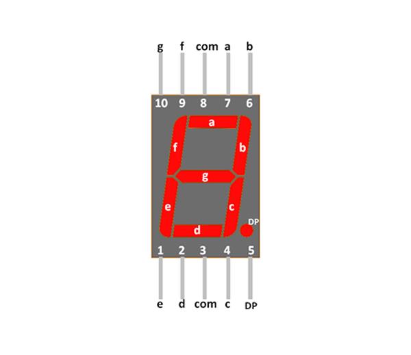
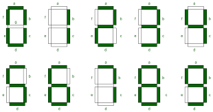
A seven segment display can be used to display a decimal 0 – 9 digit by activating the correct
segments as shown in the figure below. Note particularly when the b-segment (the top right
hand vertical segment) will turn ON or OFF.
(i) Complete the truth table that
will indicate the status of the b segment when a four-bit
BCD code is put on the display. Assume that a 1 output will mean that the segment is turned
ON and a 0 output implies that the segment remains OFF.
(4)
D
C
B
A
b Segment
0
0
0
0
0
0
0
1
0
0
1
0
0
0
1
1
0
1
0
0
0
1
0
1
0
1
1
0
0
1
1
1
1
0
0
0
1
0
0
1
1
0
1
0
1
0
1
1
1
1
0
0
1
1
0
1
1
1
1
0
1
1
1
1
7
(ii) Use your truth table to construct a K-map and simplify the logic needed to
produce the
b-segment.
(4)
/B/A
/BA
BA
B/A
/D/C
/DC
DC
D/C
(iii) Implement this logic using logic gates
(2)
8

 Question 4
[15]
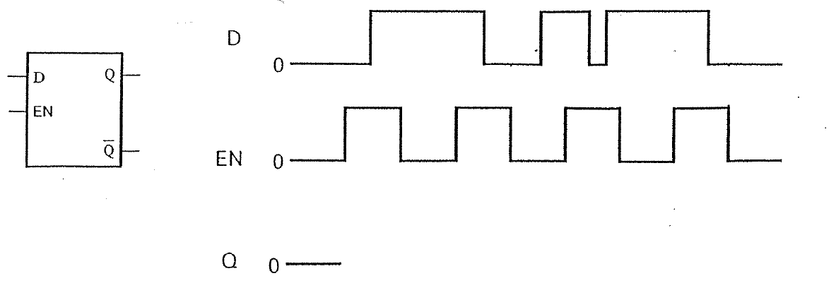
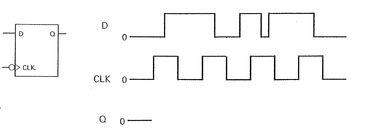
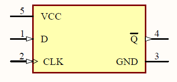
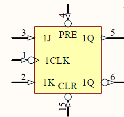
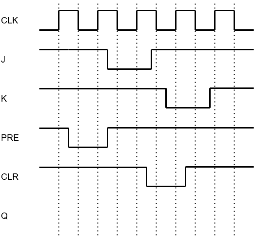
(a) For each of the flip flops below complete the timing diagram by adding the timing for the
Q output. In each case assume that Q is initially LO.
(i)
(2)
(ii)
(2)
9

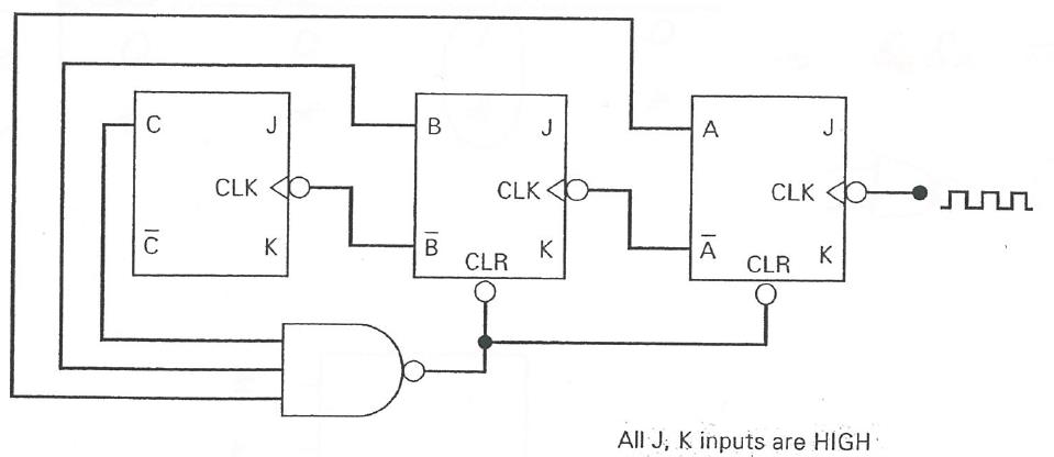
(b) Study the circuit of the counter below and answer the questions below. You can assume
that all J=K=1.
(i) On what output code (CBA) will the counter reset ?
(1)
(ii) What code will the counter reset to ?
(1)
(iii) Assume that the counter has just reset to the code in (ii). Sketch a timing diagram
showing the CLK pulse as well as the outputs A, B and C for successive further CLK pulses
until the counter repeats.
(3)
CLK
A
B
C
(iv) Determine the counting sequence that the counter will cycle through.
(2)
(iv) What is the MOD number of this counter ?
(1)
10
(c) Explain the problem that will be encountered when using an asynchronous counter with
moderately high speed input signals. Base your answer on the use of an 8-bit asynchronous
counter and assume that each flip flop element has a propagation delay of approximately 20
ns.
(3)
11
Question 5
(15)
You must design a counter that can operate either as a MOD 3 counter (states BA counting
through 00-01-10) or as a MOD 4 counter (state 11 the additional state). It is driven by an
external clock signal (CLK) and the counter should switch between the two types of counters
depending on the state of a control input C. With C=0 the counter must be in the MOD 3
counter mode and with C=1 in the MOD 4 counter mode. Both counters should count UP
when a direction bit D = 1 and DOWN when D = 0. If the counter should be in the 11 state
(MOD 4) and the control bit C changes to 0 (MOD 3 mode) the counter should then go to
the correct MOD 3 state as determined by the direction control bit.
(i) The state transition diagram for this design is shown below. Complete this diagram by
inserting the values of D and C required for each transition.
(5)
00
D
C
D
C
D
C
D
C
D
C
D
C
01
11
D
C
D
C
D
C
D
C
10
12
(ii) Now complete the excitation table below, filling in the values of the next state Bn+=1An+1
for each present state BnAn.
(5)
(iii) Assume that you are required to design this counter based on J-K flip flops. Complete
the excitation table for required values for JA and KA, the inputs into the flip flop controlling
the LSB.
(5)
D
C
Bn
An
Bn+1
An+1
JA
KA
0
0
0
0
0
0
0
1
0
0
1
0
0
0
1
1
0
1
0
0
0
1
0
1
0
1
1
0
0
1
1
1
1
0
0
0
1
0
0
1
1
0
1
0
1
0
1
1
1
1
0
0
1
1
0
1
1
1
1
0
1
1
1
1
*****
13
14
EEEN202 Test 2
12th June 2021
9:30am – 11:00am in MCLT101
Open Book: Written and printed notes are allowed.
Calculators also permitted.
Total: 50 Marks
Total time: 90 minutes
Student Name
Student Number
Instructions:
Please read all instructions carefully.
Answer questions on these sheets. Use the back of the sheets if you need
more space.
The test is in two parts, part A and part B. You are to answer only one of the
two questions in part A and all of the questions in Part B.
Part A, Digital electronics and Logic
Answer either Question 1 or Question 2
Question 1 (16 marks total)
On an industrial assembly line the output of four sensors (S3, S2, S1 and S0) are used to
monitor the presence of an object. The sensors all have a binary output and wil produce a
HI signal when the object is detected. A fault condition on the production line is indicated
when more than one of the sensors detect the object at the same time. However, the
system is designed so that S3 and S0 wil never be HI at the same time and similarly S2 and
S1 wil never be HI at the same time. You must now design a logic circuit that wil put the
output Z in a HI state when a fault condition is detected on the line.
(a) Complete the truth table below, showing the relationship between the sensor outputs
and the output of the logic circuit.
(4 marks)
S3
S2
S1
S0
Z
0
0
0
0
0
0
0
1
0
0
1
0
0
0
1
1
0
1
0
0
0
1
0
1
0
1
1
0
0
1
1
1
1
0
0
0
1
0
0
1
1
0
1
0
1
0
1
1
1
1
0
0
1
1
0
1
1
1
1
0
1
1
1
1
(b) Use your truth table to construct the K-map and simplify. Complete the K-map below
and clearly show your simplification and the resultant logic equation.
(4 marks)
/S1./S0
/S1.S0
S1.S0
S1./S0
/S3./S2
/S3.S2
S3.S2
S3./S2
(c) You must now implement this logic, but it is given that you have only 2-input logic gates
available and need to implement your circuit using as few logic gates as possible. Sketch
your suggested logic circuit.
(4 marks)
(d) You must now implement the same logic, but use an 8:1 MUX. Clearly show what inputs
wil be connected to each of the select inputs as wel as the data inputs on the MUX below.
(4 marks)
I7
I6
I5
I4
Z
I3
I2
I1
I0 S2 S1 S0
Question 2 (16 marks total)
You have to design a synchronous 3-bit (CBA) up/down counter that can count up through
the states (001) → (010) → (100) → (101) and recycles. The counter should contain a
direction input which forces it to count down on a LO control signal. It should also contain a
stop/go control that wil freeze the counter when this signal is HI. If any unused states are
encountered, the counter should go to (001).
(a) Sketch the state transition diagram for this counter.
(4marks)
(b) Neglect the stop/go control signal described above and complete the excitation table
below for this counter using D flip-flops.
(4 marks)
Present
Next
Required
D
C
B
A
C
B
A
DC
DB
DA
0
0
0
0
0
0
0
1
0
0
1
0
0
0
1
1
0
1
0
0
0
1
0
1
0
1
1
0
0
1
1
1
1
0
0
0
1
0
0
1
1
0
1
0
1
0
1
1
1
1
0
0
1
1
0
1
1
1
1
0
1
1
1
1
(c) Use a K-map and determine the logic required for DA. Complete the K-map below and
clearly show your simplification and the resultant logic equation.
(4 marks)
/B./A
/B.A
B.A
B./A
/D./C
/D.C
D.C
D./C
(d) Show how DA can be implemented using an 8 :1 MUX. Clearly show what inputs wil be
connected to each of the select inputs as wel as the data inputs on the MUX below.
(4 marks)
I7
I6
I5
I4
Z
I
3
I2
I1
I0 S2 S1 S0
Part B, Microprocessors, ADCs, DACs and memory
Answer all questions.
Question 3 (12 marks total) Microprocessors
(a) Briefly describe the function of the Arithmetic Logic Unit (ALU).
(2 marks)
(b) With regard to the 8051 series microprocessor, explain the difference between the RET
and RETI instructions.
(2 marks)
(c) Briefly describe the difference between a microprocessor and a microcontrol er.
(2 marks)
(d) Describe the differences between the Pol ing and Interrupt driven approaches and the
advantages/ disadvantages.
(6 marks)
Question 4 (12 marks total) ADC and DAC
(a) Sketch a diagram of a feedback type Analogue to Digital Converter and describe the
function of each of the key parts.
(6 marks)
(b) Briefly explain the key principle behind the Successive Approximation Convertor in how
it goes about generating the guess values.
(2 marks)
(c) A 12-bit ADC has an input voltage range of 0 to +5V
i. What is the resolution?
(2 marks)
ii. What would be the decimal and binary output values for an input voltage of 3.72V
(2 marks)
Question 5 (10 marks total) Memory
(a) A typical computer system wil use a combination of SRAM and DRAM. Briefly describe
the differences between these two types of memory and the typical purpose they are used
for.
(4 marks)

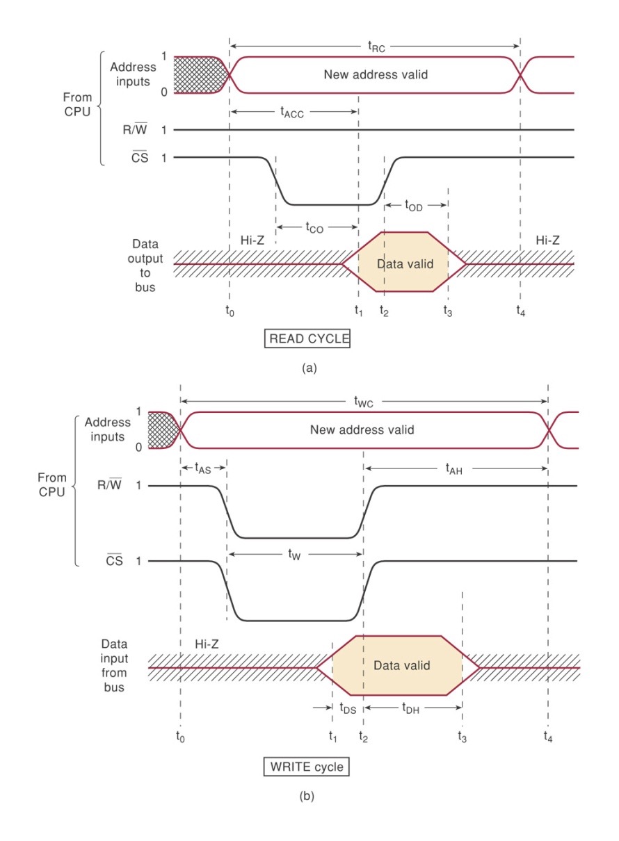
(b) The diagram below shows the timing and operation of various signals during a memory
read cycle. Describe the signals and the steps that the microprocessor and the memory each
Typical timing for static RAM: (a) read cycle; (b) write cycle.
undergo.
(6 marks)
EEEN 202
Test 1
April 2022
Instructions:
Attempt all questions.
You have until
Wednesday 27th April at 3 pm to complete and submit the test.
Your answers can be neatly handwritten, and any figures or schematics can be hand
drawn. If you prefer you can type your answers and/or submit electronic drawings.
It is strongly suggested that you first do a draft version, and then when satisfied
complete your final, neat version.
Turn your answers sheets into a single pdf document and submit under “Test 1” on
the wiki.
The test should be completed individually, but you can use resources such as your
class notes, recorded lectures or even the internet to help you. Use appropriate
component datasheets as available on the web to help you when needed. Please
bear in mind though, this test is time limited and accessing these resources may
consume valuable writing time.
The test consists of 6 questions with 10 marks per question. A total of 60 Marks.
Estimated time for completion: Estimated test time 60 minutes with a total of
60 Marks, therefore, 1 minute per mark. This gives 1 hour of leeway for computer
issues and submission.
1.
Algebraic simplification
a. Simplify the following expression using Boolean algebra:
𝑋 = 𝐴̅. 𝐵. 𝐶 + 𝐴. 𝐵̅. 𝐶̅ + 𝐴̅. 𝐵̅. 𝐶̅ + 𝐴. 𝐵̅. 𝐶 + 𝐴. 𝐵. 𝐶
(4)
b. Use the Karnaugh map below to minimise the following sum-of-
products expression:
𝑌 = 𝐵̅. 𝐶̅. 𝐷
̅ + 𝐴̅. 𝐵. 𝐶̅. 𝐷̅ + 𝐴. 𝐵. 𝐶̅. 𝐷̅ + 𝐴̅. 𝐵̅. 𝐶. 𝐷 +
𝐴. 𝐵̅. 𝐶. 𝐷 + 𝐴̅. 𝐵̅. 𝐶. 𝐷
̅ + 𝐴̅. 𝐵. 𝐶. 𝐷̅ + 𝐴. 𝐵. 𝐶. 𝐷̅ +
𝐴. 𝐵̅. 𝐶. 𝐷
̅
(6)
𝑌 =
𝐶̅. 𝐷
̅
𝐶̅. 𝐷
𝐶. 𝐷
𝐶. 𝐷
̅
𝐴̅. 𝐵̅
𝐴̅. 𝐵
𝐴. 𝐵
𝐴. 𝐵̅
2.
De Morgan’s law.
a. Draw up a truth table for an exclusive OR (XOR) gate.
(1)
b. Write down the logic function for the XOR gate.
(1)
c. Show how this gate can be constructed from inverters and OR gates.
(4)
d. You find out that you only have NAND gates available. Show how you
can construct a XOR gate from NAND gates only.
(4)
3.
Karnaugh map design.
You need to design a logic circuit that will check a 4-bit BCD code and produce
a logic 1 output when the decimal equivalent of the code is a prime number
(remember 0 and 1 are not prime numbers).
a. Draw up a truth table for your system.
(2)
b. Use a Karnaugh map (k-map) to simplify the logic.
(4)
c. Sketch the design of your logic circuit.
(4)
4.
Counter design.
a. Sketch a logic diagram to show how you can use J-K flip-flops to
construct a 3-bit asynchronous down counter.
(3)
b. Calculate the maximum frequency at which this counter will reliably
operate if the propagation delay of a J-K flip-flop is given as 𝑡𝑃𝐿𝐻 =
16 ns and 𝑡𝑃𝐻𝐿 = 24 ns.
(2)
c. Show how you can modify the design in Question 4a to operate as a
synchronous counter, with the ability to count both down and up
(count up on an active low (logic 0) control input). Will there be any
propagation delay in this counter?
(5)
5.
You are required to design the logic needed to drive a stepper motor through
the counting sequence in wave drive mode. The circuit should have an input
D which changes the rotation direction of the stepper motor. The sequence,
when D = 1, with W4 as the MSB and W1 as the LSB is 1000 -> 0001 -> 0100
-> 0010. You do NOT need to make provision to stop the motor. Feel free to
use any sequential or combinatorial logic elements. Clearly show your design
process:
a. The state transition diagram for the 2-bit synchronous Gray code
counter.
(1)
b. The transition table diagrams from current to the next flip-flop state.
Show the flip-flop inputs required to transition flip-flop states.
(2)
c. The logic simplification process for the synchronous counter. (4)
d. The output logic that converts the output of the 2-bit Gray code
counter to the four motor windings W1-4.
(1)
e. Sketch the logic diagram that will represent your design.
(2)
6.
A logic circuit is used to compare the magnitudes of two 2-bit binary
numbers, AB and CD. The circuit has two outputs, E and F and functions in
such a way that:
• The O/P E will be logic 1 whenever AB = CD and logic 0 when AB ≠ CD.
• The O/P F will be logic 1 when CD > AB and logic 0 when CD < AB.
• The O/P F will be in a ‘don’t care’ state (X) when output E is logic 1 (AB = CD).
A
E
B
C
F
D
You must now design the logic to implement the output F.
a. Draw up a truth table that relates the inputs ABCD to the output F. (3)
b. Show how you will implement this logic for F on a single 8:1 MUX.
(3)
c. Show how you will implement this logic for F on a 4:1 MUX.
(4)
EEEN 202
Test 1
April 2022
Instructions:
Attempt all questions.
You have until
Wednesday 27th April at 3 pm to complete and submit the test.
Your answers can be neatly handwritten, and any figures or schematics can be hand
drawn. If you prefer you can type your answers and/or submit electronic drawings.
It is strongly suggested that you first do a draft version, and then when satisfied
complete your final, neat version.
Turn your answers sheets into a single pdf document and submit under “Test 1” on
the wiki.
The test should be completed individually, but you can use resources such as your
class notes, recorded lectures or even the internet to help you. Use appropriate
component datasheets as available on the web to help you when needed. Please
bear in mind though, this test is time limited and accessing these resources may
consume valuable writing time.
The test consists of 6 questions with 10 marks per question. A total of 60 Marks.
Estimated time for completion: Estimated test time 60 minutes with a total of
60 Marks, therefore, 1 minute per mark. This gives 1 hour of leeway for computer
issues and submission.
1.
Algebraic simplification
a. Simplify the following expressions using Boolean algebra:
𝑅 = 𝐴
̅ ̅. 𝐵
̅ ̅
̅ .̅̅𝐶
̅ ̅
𝑇 = (𝑀
̅̅̅̅+
̅̅̅𝑁̅
̅ )
̅ .̅ (
̅̅𝑀̅
̅̅̅ +
̅̅̅ 𝑁
̅̅ )
̅̅
(4)
b. Use the Karnaugh map below to minimise the following sum-of-
products expression:
𝑌 = 𝐵̅. 𝐶̅. 𝐷
̅ + 𝐴̅. 𝐵. 𝐶̅. 𝐷̅ + 𝐴. 𝐵. 𝐶̅. 𝐷̅ + 𝐴̅. 𝐵̅. 𝐶. 𝐷 +
𝐴. 𝐵̅. 𝐶. 𝐷 + 𝐴̅. 𝐵̅. 𝐶. 𝐷
̅ + 𝐴̅. 𝐵. 𝐶. 𝐷̅ + 𝐴. 𝐵. 𝐶. 𝐷̅ +
𝐴. 𝐵̅. 𝐶. 𝐷
̅
(6)
𝑌 =
𝐶̅. 𝐷
̅
𝐶̅. 𝐷
𝐶. 𝐷
𝐶. 𝐷
̅
𝐴̅. 𝐵̅
𝐴̅. 𝐵
𝐴. 𝐵
𝐴. 𝐵̅
2.
De Morgan’s law.
a. Draw up a truth table for an exclusive OR (XOR) gate.
(1)
b. Write down the logic function for the XOR gate.
(1)
c. Show how this gate can be constructed from inverters and OR gates.
(4)
d. You find out that you only have NAND gates available. Show how you
can construct a XOR gate from NAND gates only.
(4)
3.
Karnaugh map design.
You need to design a logic circuit that will check a 4-bit BCD code and produce
a logic 1 output when the decimal equivalent of the code is a prime number
(remember 0 and 1 are not prime numbers).
a. Draw up a truth table for your system.
(2)
b. Use a Karnaugh map (k-map) to simplify the logic.
(4)
c. Sketch the design of your logic circuit.
(4)
4.
Counter design.
a. Sketch a logic diagram to show how you can use D flip-flops to
construct a 3-bit asynchronous down counter.
(3)
b. Calculate the maximum frequency at which this counter will reliably
operate if the propagation delay of a J-K flip-flop is given as
𝑡𝑃𝐿𝐻 = 𝑡𝑃𝐻𝐿 = 21 ns typical and 𝑡𝑃𝐿𝐻 = 𝑡𝑃𝐻𝐿 = 35 ns maximum.
(2)
c. Show how you can modify the design in Question 4a to operate as a
synchronous counter, with the ability to count both down and up
(count up on an active low (logic 0) control input). Will there be any
propagation delay in this counter?
(5)
5.
You are required to design the logic needed to drive a stepper motor through
the counting sequence in wave drive mode. The circuit should have an input
G which stops the rotation of the stepper motor. The sequence, when G = 1,
with W4 as the MSB and W1 as the LSB is 1000 -> 0001 -> 0100 -> 0010. You
do NOT need to make provision to change direction of the motor. Feel free
to use any sequential or combinatorial logic elements. Clearly show your
design process:
a. The state transition diagram for the 2-bit synchronous Gray code
counter.
(1)
b. The transition table diagrams from current to the next flip-flop state.
Show the flip-flop inputs required to transition flip-flop states.
(2)
c. The logic simplification process for the synchronous counter. (4)
d. The output logic that converts the output of the 2-bit Gray code
counter to the four motor windings W1-4.
(1)
e. Sketch the logic diagram that will represent your design.
(2)
6.
A logic circuit is used to compare the magnitudes of two 2-bit binary
numbers, AB and CD. The circuit has two outputs, E and F and functions in
such a way that:
• The O/P E will be logic 1 whenever AB = CD and logic 0 when AB ≠ CD.
• The O/P F will be logic 1 when CD > AB and logic 0 when CD < AB.
• The O/P F will be in a ‘don’t care’ state (X) when output E is logic 1 (AB = CD).
A
E
B
C
F
D
You must now design the logic to implement the output F.
a. Draw up a truth table that relates the inputs ABCD to the output F. (3)
b. Show how you will implement this logic for F on a single 8:1 MUX.
(3)
c. Show how you will implement this logic for F on a 4:1 MUX.
(4)
EEEN 202
Test 2
June 2022
Instructions:
Attempt all questions.
You have until
Thursday 2nd June at 3 pm to complete and submit the test.
Your answers can be neatly handwritten, and any figures or schematics can be hand
drawn. If you prefer you can type your answers and/or submit electronic drawings.
It is strongly suggested that you first do a draft version, and then when satisfied
complete your final, neat version.
Turn your answers sheets into a single pdf document and submit under “Test 2” on
the wiki.
The test should be completed individually, but you can use resources such as your
class notes, recorded lectures or even the internet to help you. Use appropriate
component datasheets as available on the web to help you when needed. Please
bear in mind though, this test is time limited and accessing these resources may
consume valuable writing time.
The test consists of 6 questions with 10 marks per question. A total of 60 Marks.
Estimated time for completion: Estimated test time 60 minutes with a total of
60 Marks, therefore, 1 minute per mark. This gives 1 hour of leeway for computer
issues and submission.
1.
Architecture
a. What are the two main computer architectures used in embedded
systems. What is the major difference between them?
(2)
b. Which of these architectures is used in the AT89C51AC3 (8051)?
(1)
c. If you wanted to store the value 0xFE, how would you do this in the
Keil uVision IDE?
i. into register R0 using assembly code?
(1)
ii. into a variable located in the internal data memory using C?
(1)
d. In the AT89C51AC3 (8051 series) microprocessor, describe what
happens when the ACALL instruction is executed. What happens to the
program counter and stack pointer during this operation?
(2)
e. What location does value of the stack pointer describe?
(1)
f. What assembly instruction can be used to place data onto the stack?
(1)
g. What assembly instruction can be used to remove data from the
stack?
(1)
2.
Memory
a. What is the space in bytes that is reserved to store each service routine
for the interruptions sources in the AT89C51AC3? If a service routine
of an interrupt source is larger than the available space, how must you
allocate it in the non-volatile memory (which assembly instruction(s)
could be used)?
(3)
b. What is internal data memory structure of the 8051 microcontroller?
Explain each memory part. Which area is bit addressable? which area
is only accessible using direct addressing? Which area is only
accessible using indirect addressing?
(3)
c. Some 8-bit wide SRAM is connected to the data, address, and control
buses of a microprocessor. Sketch a typical timing diagram showing
how the microprocessor writes a word of data to the SRAM. You
should specifically indicate the following lines:
i. Data bus
ii. Address bus
iii. Chip Select line
iv. Read/Write line
(4)
3.
Data Display.
There are two methods of displaying ASCII numerical data on a 44780 LCD
module (the LCD module used in the labs), depending on if the data is stored
in binary or binary coded decimal format.
a. What is an advantage and a disadvantage of storing a numerical value
on the 8051 in BCD encoding when compared to straight binary
encoding?
(2)
b. What are the ASCII values of the numerals between 0 and 9?
(1)
c. What does the DA instruction do on the 8051?
(1)
d. An operation must be performed directly before the DA instruction on
the 8051. What operation is it? Which instructions could be used to
achieve this operation?
(1)
e. Show how ASCII numerical data could be displayed on the 44780 LCD,
if R0 contains a number between 0x00 and 0x63 which is stored in
straight binary encoding.
(3)
f. Show how ASCII numerical data could be displayed on the 44780 LCD,
if R1 contains a number between 0x00 and 0x63 which is stored in BCD
encoding.
(2)
4.
Analog to digital conversion.
A thermocouple (temperature sensor) has an output of 0 to 46 mV over a
measuring range of 0 – 800 °C.
a. Calculate by how much the output of a 12-bit ADC with a 0 – 5 V input
range would change over the full input range of the thermocouple.
(3)
b. What would be the temperature resolution of this system?
(2)
c. Would this be a practical system, why or why not?
(2)
d. What would be the resolution if a 16-bit ADC was used?
(2)
e. What can be done to improve this situation?
(1)
5.
Writing assembly code.
Design a piece of software for the AT89C51AC3 (8051) in Assembly language
that executes an addition operation between the contents of the memory
location whose address is given by the content of the R0 register and the
content of the memory location whose address is 7Ah. Next, subtract the
content of the R4 register. Swap the order of the least significant and most
significant nibbles of the result of the subtraction. The result must be stored
in the R7 register of register bank 3.
(10)

6.
Write assembly language code that enables the AT89C51AC3 ADC when the
microcontroller is turned on. Using ORL, begin a conversion with analog input
7 (AN7) selected, the CPU noise must be minimized therefore the conversion
must be made in precision mode (using all 10-bits of the ADC). The ADC result
must be bit addressable and stored in little-endian format (that is the least
significant byte is stored at the smallest address). Retrieve the ADC result
and store it beginning at address 0x20.
(10)
EEEN 202
Test 2 Resit
June 2022
Instructions:
Attempt all questions.
You have until
Thursday 9th June at 4:30 pm to complete and submit the test.
Your answers can be neatly handwritten, and any figures or schematics can be hand
drawn. If you prefer you can type your answers and/or submit electronic drawings.
It is strongly suggested that you first do a draft version, and then when satisfied
complete your final, neat version.
Turn your answers sheets into a single pdf document and submit under “Test 2” on
the wiki.
The test should be completed individually, but you can use resources such as your
class notes, recorded lectures or even the internet to help you. Use appropriate
component datasheets as available on the web to help you when needed. Please
bear in mind though, this test is time limited and accessing these resources may
consume valuable writing time.
The test consists of 29 questions with marks as indicated. A total of 80 Marks.
Estimated time for completion: Estimated test time 60 minutes, the multichoice
and short answer questions should be quick to complete leaving more time for the
long answer questions. This gives 1 hour of leeway for computer issues and
submission.
1.
The AT89C51AC3 is ‘binary compatible’ with which popular microcontroller?
(1)
2.
a. What high-level computer architecture makes use of a shared data
and program memory?
(1)
b. What high-level computer architecture makes use of separate data
and program memories?
(1)
c. Which of the architectures from questions 2A and 2B does the 8051
employ?
(1)
d. What does CISC stand for, and is the 8051 an example of a CISC
system?
(1)
3.
In a standard 8051, how many clock cycles result in one machine cycle?
(1)
4.
a. Given a 40 MHz crystal, find the time (in μs) required for one machine
cycle.
(2)
b. Given a 12 MHz crystal, find the time (in μs) required for one machine
cycle.
(2)
5.
a. In a CPU, what does ALU stand for?
(1)
b. In the 8051, what is an alternative name for Register A?
(1)
c. How many bits is Register A?
(1)
d. What register holds the address of the next instruction to be
executed?
(1)
6.
a. What is 0d16 in hexadecimal?
(1)
b. What is a larger numerical value: 0d128 or 0xFF?
(1)
c. What is a smaller numerical value: 0b10000000 of 0xFF?
(1)
d. Circle or underline the lower nibble of this 8051 byte: 0b10101010
(1)
7.
a. On the 8051, what does the NOP instruction do?
(1)
b. On the 8051, what does the INC instruction do?
(1)
8.
Multiple choice (circle one of a-d): On the 8051, when MOV A,B is called,
which of the following occurs?
a. The contents of B are moved to A, with B’s contents being cleared after
this operation.
b. The contents of a A are moved to B, with A’s contents being cleared
after this operation.
c. The contents of B are moved to A, with B’s contents being retained
after this operation.
d. The contents of a A are moved to B, with A’s contents being retained
after this operation.
(1)
9.
Multiple choice (circle one of a-d): On the 8051, which of the following
instructions is directly associated with a subroutine call?
a. LJMP
b. SJMP
c. ACALL
d. INC
(1)
10.
In a hex file, what is the role of the checksum, and (in an 8051 hex file) how
is it calculated?
(1)
11.
a. How many register banks does the 8051 have?
(1)
b. By default, which register bank is occupied by the 8051’s stack?
(1)
c. When looking at the 8051’s memory map, what does SFR stand for?
(1)
d. What addressing mode is used by the following instruction?
MOV A, R7
(1)
12.
a. What instruction is used to add data to the stack?
(1)
b. What instruction is used to remove data from the stack?
(1)
c. What register (containing the last used location of the stack) is
incremented/decremented by the instructions in (12a) and (12b)?
(1)

13.
Timer mode information and details about the TMOD register are provided.
Write code that sets Timer 0 to Mode 1 and Timer 1 to Mode 3. Assume that
TMOD holds other values that must not be overwritten.
(3)

14.
Information about the TCON register is provided below. Assume that TCON
holds other values that must not be overwritten. Write code that
sequentially fulfils the following three steps:
Step 1: Stop Timer 0.
Step 2: Clear Timer 0’s overflow flag.
Step 3: Start Timer 0.
(3)
15.
Using information about the TMOD and TCON registers provided above,
write code that sequentially fulfils the following steps. Assume that your
registers begin in a zeroed out state.
Step 1: Set Timer 1 as a counter in Mode 2.
Step 2: Clear the TH1 register (TH1 is the register that holds counter values).
Step 3: Start Timer 1.
(3)
16.
With a 12 MHz clock frequency on the AT89C51AC3, what would be the
reload value of a timer to generate an interrupt or overflow once per
millisecond.
(1)
17.
With a 12 MHz clock frequency on the AT89C51AC3, what would be the
reload value of a timer to generate an interrupt or overflow once every
25 ms.
(1)
18.
Briefly describe the advantages of an interrupt-driven approach compared
to a blocking/polling approach.
(2)
19.
a. In relation to interrupts, what does ISR stand for?
(1)
b. What timer condition triggers a Timer-related interrupt?
(1)
c. What two pin states can be used to trigger an external interrupt?
(1)
d. On the 8051, INT0 and INT1 are what type of interrupt?
(1)
20.
8051 assembly language programs often contain variations of the following
code. Briefly explain the point of the ORG and LJMP instructions as they
relate to interrupt vector tables.
ORG 0000h
LJMP MAIN
// ISR CODE HERE
ORG 0030h
MAIN:
// MORE CODE HERE
(2)

21.
Fill in the blanks
with 8051 assembly language code that fulfils the behaviour
described in the comments. Each blank (5 blanks total) has a corresponding
comment that should be realised in code. Details about the IEN0 register are
below. Consult prior pages’ details about other registers.
ORG 0000H
LJMP MAIN
;— ISR: Interrupt 1, toggles LED when new interrupt arrives.
____________ ;directive to place ISR code at INT1 vector table location (0013H)
____________ ;Toggle Port 1 pin 3 (CPL instruction)
____________ ;Instruction to reset PC and clear interrupt flags
;Set up interrupts at a ROM location past vector table
ORG 0030H
MAIN:
____________ ;In TCON, set Interrupt 1 to falling edge triggered
____________ ;In IEN0, enable all interrupts and INT1. You may
;assume that IEN0 is initially zeroed out.
IDLE: SJMP IDLE
;Other code could go here. Idle main CPU for now.
END
(5)

22.
Why do we need to call PSIDLE when using the ADC in precision mode?
(1)
23.
Write assembly language code that fulfils the following steps. Write one line
of code per step.
Step 1: From standby mode, enable the ADC.
Step 2: Using ORL, begin a conversion; all 10 bits of the conversion will be
needed, so CPU noise must be minimised.
(2)
24.
Multiple choice. Circle one of A-D. Which of the following is not true about
the AT89C51AC3?
a. It has three 16-bit timers
b. It has two 10-bit ADCs
c. It has two external interrupt pins
d. It has one watchdog timer
(1)
25.
The initial contents of Register A are 0b11001100. What are the contents of
register A after the execution of an ORL instruction against A with an operand
of 0b00110011?
(2)
26.
The initial contents of Register A are 0b11111111. What are the contents of
register A after the execution of an ANL instruction against A with an operand
of 0b00100000?
(2)
27.
The A register has an initial value of 0b00000100
What are the register’s contents after executing the following code?
RR A
RR A
ANL A, #10000011B
(2)
28.
a. Sketch a basic design for a 4-bit flash converter that will convert
voltages in the input range 0 to 8 V.
(3)
b. Indicate the resistor values that you will use to create the desired
reference voltages.
(2)
c. What will be the binary output code for an input voltage of 3.4 V?
(2)
29.
A thermocouple (temperature sensor) has an output of 0 to 46 mV over a
measuring range of 0 to 800 °C.
a. Calculate by how much the output of a 12-bit A/D converter with a
0 to 5 V input range would change over the full input range of the
thermocouple.
(3)
b. What would be the temperature resolution of this system?
(2)
c. Would this be a practical system, why or why not?
(1)
d. What would be the resolution if a 16-bit A/D was used?
(2)
e. What can be done to improve this situation?
(1)
END
EEEN202 Test
27 April 2023
Total: 44 marks
Time: 50 minutes
Student Name
Student Number
Instructions:
Attempt all questions.
Write down your answers in the spaces provided, using the tables or device
outlines as appropriate.
Question
Marks
Obtained
1
8
2
10
3
8
4
18
Total
44
%
1
Question 1
[8]
A truth table indicating the state of an output, Z, as it depends on three inputs A, B and C is
given below:
A
B
C
Z
0
0
0
0
0
0
1
1
0
1
0
0
0
1
1
0
1
0
0
0
1
0
1
1
1
1
0
1
1
1
1
1
(i) Write down the sum of products expression as represented by the truth table and then
simplify this expression.
(3)
(ii) Sketch the logic circuit that represent your simplified expression in (i)
(2)
2


(iii) Show how you will implement an OR gate A+B = Z using only NAND gates.
(3)
Question 2
[10]
A seven-segment display can be used to display a decimal 0 – 9 digit by activating the
correct segments on an LED display as shown in the figure below. Note particularly when
the b-segment (the top right-hand vertical segment) will turn ON or OFF.
(i) Complete the truth table (outline on next page) that
will indicate the status of the b
segment when a four-bit BCD code is put on the display. Assume that a 1 output will mean
that the segment is turned ON and a 0 output implies that the segment remains OFF. (4)
3

 D
C
B
A
b Segment
0
0
0
0
0
0
0
1
0
0
1
0
0
0
1
1
0
1
0
0
0
1
0
1
0
1
1
0
0
1
1
1
1
0
0
0
1
0
0
1
1
0
1
0
1
0
1
1
1
1
0
0
1
1
0
1
1
1
1
0
1
1
1
1
4
(ii) Use your truth table to construct a K-map and simplify the logic needed to
produce the
b-segment.
(4)
/B/A
/BA
BA
B/A
/D/C
/DC
DC
D/C
(iii) Implement this logic using logic gates
(2)
5
 Question 3
[8]
Study the circuit of the counter below and answer the questions below. You can assume
that all J=K=1 and that flip-flop C will always have the CLEAR input in the disabled state.
(i) On what output code (CBA) will the counter reset ?
(1)
(ii) What code will the counter reset to ?
(1)
(iii) Assume that the counter has just reset to the code in (ii). Sketch a timing diagram
showing the CLK pulse as well as the outputs A, B and C for successive further CLK pulses
until the counter repeats.
(3)
CLK
A
B
C
(iv) Determine the counting sequence that the counter will cycle through.
(2)
(iv) What is the MOD number of this counter ?
(1)
6
Question 4
(18)
You must design a counter that can operate either as a MOD 3 counter (states BA counting
through 00-01-10) or as a MOD 4 counter with 11 the additional state. It is driven by an
external clock signal (CLK) and the counter should switch between the two types of counters
depending on the state of a control input C. With C=0 the counter must be in the MOD 3
counter mode and with C=1 in the MOD 4 counter mode. Both counters should count UP
when a direction bit D = 1 and DOWN when D = 0. If the counter should be in the 11 state
(MOD 4) and the control bit C changes to 0 (MOD 3 mode) the counter should then go to
the correct MOD 3 state as determined by the direction control bit.
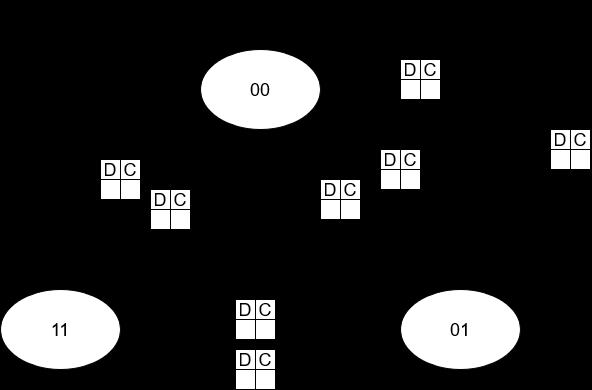
(i) The state transition diagram for this design is shown below. Complete this diagram by
inserting the values of D and C required for each transition.
(4)
00
D
C
D
C
D
C
D
C
D
C
D
C
01
11
D
C
D
C
D
C
D
C
10
7
(ii) Use the state transition diagram to complete the excitation table below, filling in the
values of the next state Bn+=1An+1 for each present state BnAn.
(3)
(iii) Assume that you are required to design this counter based on J-K flip flops. Complete
the excitation table for required values for JA and KA, the inputs into the flip flop controlling
the least significant bit of the code.
(5)
D
C
Bn
An
Bn+1
An+1
JA
KA
0
0
0
0
0
0
0
1
0
0
1
0
0
0
1
1
0
1
0
0
0
1
0
1
0
1
1
0
0
1
1
1
1
0
0
0
1
0
0
1
1
0
1
0
1
0
1
1
1
1
0
0
1
1
0
1
1
1
1
0
1
1
1
1
8
(iv) Show how you can
implement the logic for JA using a generic 4:1 MUX. Take care to
show what the inputs to S1 and S0 will be and what data needs to be connected to the inputs
I0 to I3 to enable the correct operation of the MUX.
(4)
I3
I2
Z
I
1
I0 S1
S0
(v) What will be the simplest implementation of the logic for KA ?
(2)
****End of Test*****
9
EEEN 202
Test 2
June 2023
Name:
Student ID:
Instructions:
Attempt all questions.
You have
40 minutes to complete the test.
The test is
closed book and should be completed individually.
You may use a calculator, but not your mobile phone.
Your answers can be neatly handwritten, and you should staple any additional
pages used to the test, placing your name on all pages.
The test consists of 4 questions with 10 marks per question. A total of 40 Marks.
1.
Architecture
a. What are the two main computer architectures used in embedded
systems. What is the major difference between them?
(2)
b. Which of these architectures is used in the AT89C51AC3 (8051)?
(1)
c. When looking at the 8051’s memory map, what does SFR stand for?
(1)
d. What addressing mode is used by the following instruction?
MOV A, R0
(1)
e. In the AT89C51AC3 (8051 series) microprocessor, describe what
happens when the ACALL instruction is executed. What happens to the
program counter and stack pointer during this operation?
(2)
f. What location does value of the stack pointer describe?
(1)
g. What assembly instruction can be used to place data onto the stack?
(1)
h. What assembly instruction can be used to remove data from the
stack?
(1)
2.
Memory
a. What is the space in bytes that is reserved to store each interrupt
service routine in the AT89C51AC3? If a service routine of an interrupt
is larger than the available space, how must you allocate it in the non-
volatile memory (which assembly instruction(s) could be used)?
(3)
b. What is internal data memory structure of the 8051 microcontroller?
Explain each memory part. Which area is bit addressable? which area
is only accessible using direct addressing? Which area is only
accessible using indirect addressing?
(3)
c. Some 8-bit wide SRAM is connected to the data, address, and control
buses of a microprocessor. Sketch a typical timing diagram showing
how the microprocessor writes a word of data to the SRAM. You
should specifically indicate the following lines:
i. Data bus
ii. Address bus
iii. Chip Select line
iv. Read/Write line
(4)
*** BLANK PAGE FOR WORKING ***
3.
Timers.
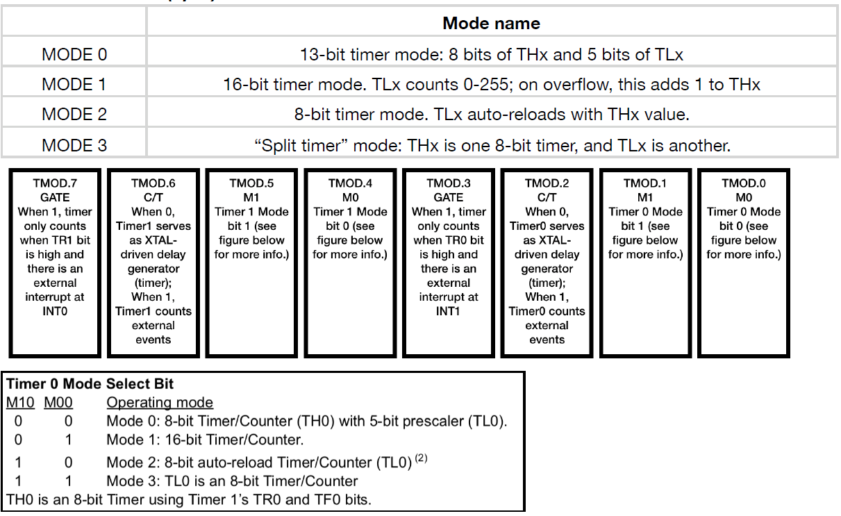
Timer mode information and details about the TMOD register are provided.
Write code that sets Timer 0 to Mode 1 and Timer 1 to Mode 2. Assume that
TMOD holds other values that must not be overwritten.
Mode Name
Mode 0
13-bit timer mode: 8-bits of THx and 5-bits of TLx
Mode 1
16-bit timer mode: TLx counts 0-255; on overflow this adds 1 to THx.
Mode 2
8-bit timer mode. TLx auto-reloads with THx value
Mode 3
“Split timer” mode: THx is one 8-bit timer, and TLx is another.
TMOD Register TMOD (089h)
TMOD.7
GATE When 1, timer only counts when TR1 bit is high and INT1# pin is
high.
TMOD.6
C/T
When 0, Timer 1 operates as a timer;
When 1, Timer 1 operates as a counter.
TMOD.5
M1
Timer 1 Mode select bit (see below)
TMOD.4
M0
Timer 1 Mode select bit (see below)
TMOD.3
GATE When 1, Timer 0 only counts when TR0 bit is high and INT0# pin is
high.
TMOD.2
C/T
When 0, Timer 0 operates as a timer;
When 1, Timer 0 operates as a counter.
TMOD.1
M1
Timer 0 Mode select bit (see below)
TMOD.0
M0
Timer 0 Mode select bit (see below)
Timer Mode Select Bits
M1
M0
Operating Mode
0
0
Mode 0: 8-bit Timer/Counter (TH0) with 5-bit prescaler (TL0)
0
1
Mode 1: 16-bit Timer/Counter
1
0
Mode 2: 8-bit auto-reload Timer/Counter (TL0)
1
1
Mode 3: TL0 is an 8-bit Timer/Counter
TH0 is an 8-bit Timer/Counter using Timer 1’s TR0 and TF0 bits
(3)
Information about the TCON register is provided below. Assume that TCON
holds other values that must not be overwritten. Write code that
sequentially fulfils the following three steps:
Step 1: Stop Timer 0.
Step 2: Clear Timer 0’s overflow flag.
Step 3: Start Timer 0.
TCON Register TCON (088h)
TCON.7
TF1
Timer 1 overflow flag. 1 when overflow occurs. Must be cleared in
software; Automatically cleared when exiting ISR.
TCON.6
TR1
Timer 1 run bit. (Software controlled).
1: Start timer.
0: Stop Timer.
TCON.5
TF0
Timer 0 overflow flag. 1 when overflow occurs. Must be cleared in
software; Automatically cleared when exiting ISR.
TCON.4
TR0
Timer 0 run bit. (Software controlled).
1: Start timer.
2: Stop timer.
TCON.3
IE1
External interrupt 1 edge flag. (Hardware controlled).
1: External interrupt occurred.
0: External interrupt processed.
TCON.2
IT1
Interrupt 1 trigger type select bit.
1: Interrupt occurs on the falling edge of INT1.
0: Interrupt occurs on INT1’s level being low.
TCON.1
IE0
External interrupt 0 edge flag. (Hardware controlled).
1: External interrupt occurred.
0: External interrupt processed.
TCON.0
IT0
Interrupt 0 trigger type select bit.
1: Interrupt occurs on the falling edge of INT0.
0: Interrupt occurs on INT0’s level being low.
(3)
Using the information about the TMOD and TCON registers provided above,
write code that sequentially fulfils the following steps. Assume that your
registers begin in a zeroed out state.
Step 1: Set Timer 1 as a counter in Mode 2.
Step 2: Clear the TH1 register (TH1 is the register that holds counter values).
Step 3: Start Timer 1.
(3)
With a 12 MHz clock frequency on the AT89C51AC3, what would be the
reload value of a timer to generate an interrupt or overflow once per
millisecond.
(1)
4.
Analog to digital conversion.
A thermocouple (temperature sensor) has an output of 0 to 46 mV over a
measuring range of 0 – 800 °C.
a. Calculate by how much the output of a 12-bit ADC with a 0 – 5 V input
range would change over the full input range of the thermocouple.
(3)
b. What would be the temperature resolution of this system?
(2)
c. Would this be a practical system, why or why not?
(2)
d. What would be the resolution if a 16-bit ADC was used?
(2)
e. What can be done to improve this situation?
(1)
*** BLANK PAGE FOR WORKING ***
*** END ***
EEEN 202
Test 2 Resit
June 2023
Name:
Student ID:
Instructions:
Attempt all questions.
You have
40 minutes to complete the test.
The test is
closed book and should be completed individually.
You may use a calculator, but not your mobile phone.
Your answers can be neatly handwritten, and you should staple any additional
pages used to the test, placing your name on all pages.
The test consists of 4 questions with 10 marks per question. A total of 40 Marks.
1.
Architecture
a. What are the two main computer architectures used in embedded
systems. What is the major difference between them?
(2)
b. Which of these architectures is used in the AT89C51AC3 (8051)?
(1)
c. When looking at the 8051’s memory map, what does SFR stand for?
(1)
d. What addressing mode is used by the following instruction?
MOV A, R0
(1)
e. In the AT89C51AC3 (8051 series) microprocessor, describe what
happens when the ACALL instruction is executed. What happens to the
program counter and stack pointer during this operation?
(2)
f. What location does value of the stack pointer describe?
(1)
g. What assembly instruction can be used to place data onto the stack?
(1)
h. What assembly instruction can be used to remove data from the
stack?
(1)
2.
Memory
a. What is the space in bytes that is reserved to store each interrupt
service routine in the AT89C51AC3? If a service routine of an interrupt
is larger than the available space, how must you allocate it in the non-
volatile memory (which assembly instruction(s) could be used)?
(3)
b. What is internal data memory structure of the 8051 microcontroller?
Explain each memory part. Which area is bit addressable? which area
is only accessible using direct addressing? Which area is only
accessible using indirect addressing?
(3)
c. Some 8-bit wide SRAM is connected to the data, address, and control
buses of a microprocessor. Sketch a typical timing diagram showing
how the microprocessor reads a word of data to the SRAM. You should
specifically indicate the following lines:
i. Data bus
ii. Address bus
iii. Chip Select line
iv. Read/Write line
(4)
*** BLANK PAGE FOR WORKING ***
3.
Timers.
Timer mode information and details about the TMOD register are provided.
Write code that sets Timer 0 to Mode 2 and Timer 1 to Mode 1. Assume that
TMOD holds other values that must not be overwritten.
Mode Name
Mode 0
13-bit timer mode: 8-bits of THx and 5-bits of TLx
Mode 1
16-bit timer mode: TLx counts 0-255; on overflow this adds 1 to THx.
Mode 2
8-bit timer mode. TLx auto-reloads with THx value
Mode 3
“Split timer” mode: THx is one 8-bit timer, and TLx is another.
TMOD Register TMOD (089h)
TMOD.7
GATE When 1, timer only counts when TR1 bit is high and INT1# pin is
high.
TMOD.6
C/T
When 0, Timer 1 operates as a timer;
When 1, Timer 1 operates as a counter.
TMOD.5
M1
Timer 1 Mode select bit (see below)
TMOD.4
M0
Timer 1 Mode select bit (see below)
TMOD.3
GATE When 1, Timer 0 only counts when TR0 bit is high and INT0# pin is
high.
TMOD.2
C/T
When 0, Timer 0 operates as a timer;
When 1, Timer 0 operates as a counter.
TMOD.1
M1
Timer 0 Mode select bit (see below)
TMOD.0
M0
Timer 0 Mode select bit (see below)
Timer Mode Select Bits
M1
M0
Operating Mode
0
0
Mode 0: 8-bit Timer/Counter (TH0) with 5-bit prescaler (TL0)
0
1
Mode 1: 16-bit Timer/Counter
1
0
Mode 2: 8-bit auto-reload Timer/Counter (TL0)
1
1
Mode 3: TL0 is an 8-bit Timer/Counter
TH0 is an 8-bit Timer/Counter using Timer 1’s TR0 and TF0 bits
(3)
Information about the TCON register is provided below. Assume that TCON
holds other values that must not be overwritten. Write code that
sequentially fulfils the following three steps:
Step 1: Stop Timer 1.
Step 2: Clear Timer 1’s overflow flag.
Step 3: Start Timer 1.
TCON Register TCON (088h)
TCON.7
TF1
Timer 1 overflow flag. 1 when overflow occurs. Must be cleared in
software; Automatically cleared when exiting ISR.
TCON.6
TR1
Timer 1 run bit. (Software controlled).
1: Start timer.
0: Stop Timer.
TCON.5
TF0
Timer 0 overflow flag. 1 when overflow occurs. Must be cleared in
software; Automatically cleared when exiting ISR.
TCON.4
TR0
Timer 0 run bit. (Software controlled).
1: Start timer.
0: Stop timer.
TCON.3
IE1
External interrupt 1 edge flag. (Hardware controlled).
1: External interrupt occurred.
0: External interrupt processed.
TCON.2
IT1
Interrupt 1 trigger type select bit.
1: Interrupt occurs on the falling edge of INT1.
0: Interrupt occurs on INT1’s level being low.
TCON.1
IE0
External interrupt 0 edge flag. (Hardware controlled).
1: External interrupt occurred.
0: External interrupt processed.
TCON.0
IT0
Interrupt 0 trigger type select bit.
1: Interrupt occurs on the falling edge of INT0.
0: Interrupt occurs on INT0’s level being low.
(3)
Using the information about the TMOD and TCON registers provided above,
write code that sequentially fulfils the following steps. Assume that your
registers begin in a zeroed out state.
Step 1: Set Timer 0 as a counter in Mode 2.
Step 2: Set the reload value of the counter to 0xEB (TH0 contains the reload
value of the counter.).
Step 3: Start Timer 0.
(3)
With a 12 MHz clock frequency on the AT89C51AC3, what would be the
reload value of a timer to generate an interrupt or overflow once per
millisecond.
(1)
4.
Analog to digital conversion.
A thermocouple (temperature sensor) has an output of 0 to 36 mV over a
measuring range of 0 – 800 °C.
a. Calculate by how much the output of a 12-bit ADC with a 0 – 5 V input
range would change over the full input range of the thermocouple.
(3)
b. What would be the temperature resolution of this system?
(2)
c. Would this be a practical system, why or why not?
(2)
d. What would be the resolution if a 16-bit ADC was used?
(2)
e. What can be done to improve this situation?
(1)
*** BLANK PAGE FOR WORKING ***
*** END ***
EEEN 202
Test 1
April 2024
Name:
Student ID:
Instructions:
Attempt all questions.
You have
45 minutes to complete the test.
The test is
closed book and should be completed individually.
You may use a calculator, but not your mobile phone.
Your answers can be neatly handwritten, and you should staple any additional
pages used to the test, placing your name on all pages.
The test consists of 4 questions, with marks as indicated below, for a total of 45
Marks.
Question
Grade
Total
1
/12
2
/5
3
/14
4
/14
Total
/45
Estimated time for completion: Estimated test time 45 minutes with a total of
45 Marks, therefore, 1 minute per mark.

1.
a. Write down the Algebraic expression for De Morgan’s theorem.
(2)
b. Use De Morgan’s theorem to represent the NAND gate shown below
as another logic gate or gates.
(2)
Simplify the following expression using De Morgan’s theorem:
𝑋 = 𝐴
̅ ̅ +
̅̅̅ 𝐵̅
̅ ̅+
̅̅̅𝐶
̅ ̅
(2)
c. Use the Karnaugh map below to minimise the following sum-of-
products expression:
𝑌 = 𝐴̅. 𝐵̅. 𝐷
̅ + 𝐴̅. 𝐵. 𝐶̅. 𝐷 + 𝐴̅. 𝐵. 𝐶. 𝐷̅ + 𝐴. 𝐵. 𝐶̅. 𝐷 +
𝐴. 𝐵. 𝐶. 𝐷 + 𝐴. 𝐵̅. 𝐶̅. 𝐷
̅ + 𝐴. 𝐵̅. 𝐶. 𝐷̅
(6)
𝑌 =
𝐶̅. 𝐷
̅
𝐶̅. 𝐷
𝐶. 𝐷
𝐶. 𝐷
̅
𝐴̅. 𝐵̅
𝐴̅. 𝐵
𝐴. 𝐵
𝐴. 𝐵̅


2.
For each of the devices below sketch the timing diagram of the output that
will result from the given input conditions. Note: In all cases assume the
device is initially in the reset state.
a. Sketch 𝑄̅
[2 Marks]
b. Sketch 𝑄
[2 Marks]
c. If one of the devices above had a 𝑡𝑃𝐻𝐿 = 5 ns and a 𝑡𝑃𝐿𝐻 = 10 ns what
is the maximum frequency that the device could operate at?
[1 Mark]

3.
You must design a counter that can operate either as a MOD2 Counter (states
BA counting through 00-01) or as a MOD3 counter (states BA counting
through 00-01-11). It is driven by an external clock signal (CLK) and will switch
between the two types of counters depending on the state of a control input
C, with C=0 selecting MOD2 counter mode and C=1 the MOD3 counter mode.
Both counters should count UP when a direction bit D = 1 and DOWN when
D = 0. If the counter should be in the 11 state (MOD 3) and the control bit C
changes to 0 (MOD 2 mode) the counter should then go to the correct MOD 2
state as determined by the direction control bit.
a. The state transition diagram is shown below. Complete this diagram
by inserting the values of D and C required for each transition.
[6 Marks]
b. Now complete the excitation table below, filling in the values for the
next state 𝐵𝑛+1𝐴𝑛+1 for each present state 𝐵𝑛𝐴𝑛.
[6 Marks]
c. Assume you are required to design this counter based on D type flip-
flops. Complete the excitation table for the required values for
𝐷𝐴, and 𝐷𝐵, the inputs to the flip-flop controlling the MSB, and LSB,
respectively.
[2 Marks]
Note: I have filled in the invalid states for you
continued… P.T.O
D
C
𝐵𝑛
𝐴𝑛
𝐵𝑛+1
𝐴𝑛+1
𝐷𝐵
𝐷𝐴
0
0
0
0
0
0
0
1
0
0
1
1
0
1
0
0
0
1
0
1
0
1
1
1
1
0
0
0
1
0
1
0
1
0
1
1
1
1
0
0
1
1
0
1
1
1
1
1
X
X
1
0
0
0
0
0

4.
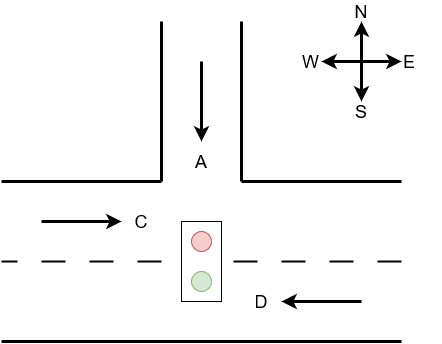
You have been asked to design a traffic light control system. Figure 1 shows
the intersection of an east-west main road and a north-south access road.
Vehicle detection sensors are placed along lane A (the access road) and lanes
C and D (the main road). The sensor outputs are low (0) when no cars are
detected and high (1) when a vehicle is present.
Figure 1: The Traffic Light System.
The intersection to the traffic light is to be controlled using the following logic:
• The east-west traffic light (E-W) will be green (1) whenever both the C and D
lanes are occupied [E-W = 𝐶. 𝐷].
• The east-west traffic light (E-W) will be green (1) whenever only one of lanes C
or D are occupied, and lane A is not occupied [E-W = (𝐶 ⊕ 𝐷). 𝐴̅].
• The north-south traffic light (N-S) will be green (1) whenever lane A is occupied
and
only
one
of
the
C
and
D
lanes
are
occupied
[N-S = 𝐴. (𝐶 ⊕ 𝐷)].
• The north-south traffic light (N-S) will be green (1) when lane A is occupied while
lanes C and D are both vacant [N-S = 𝐴. (𝐶̅. 𝐷
̅)].
• The east-west traffic light (E-W) will be green (1) when no cars are present
[E-W = 𝐴̅. 𝐶̅. 𝐷
̅].
a. Complete the truth table showing the E-W and N-S outputs from the
traffic light controller.
[8 Marks]
A
C
D
E-W
N-S
0
0
0
0
0
1
0
1
0
0
1
1
1
0
0
1
0
1
1
1
0
1
1
1
b. Implement the logic for the E-W output using an 8:1 multiplexer.
[2 Marks]
c. Simplify the expression and implement the E-W output using a 4:1
multiplexer. Note: you may need to use additional gates in your
implementation.
[4 Marks]
*** END ***
EEEN 202
Test 2
May 2024
Name:
Student ID:
Instructions:
Attempt all questions.
You have
45 minutes to complete the test.
The test is
closed book and should be completed individually.
You may use a calculator, but not your mobile phone.
Your answers can be neatly handwritten in the answer booklet, and you should
staple any additional pages used to the test, placing your name on all pages.
The test consists of 4 questions. A total of 45 Marks.
Question
Marks
Total
1
/13
2
/10
3
/12
4
/10
Total
/45
1.
a. What are the two main computer architectures used in embedded
systems, and what is the major difference between them?
[2 Marks]
b. Which of these architectures is used in the AT89C51AC3 (8051)?
[1 Mark]
c. What does ALU stand for?
[1 Mark]
d. What location does the value of the stack pointer describe?
[1 Mark]
e. In the AT89C51AC3 (8051 series) microprocessor, describe what
happens when the ACALL instruction is executed. What happens to the
program counter and stack pointer during this operation?
[2 Marks]
f. Referring to the internal data memory structure of the 8051
microcontroller:
i. Which area is bit addressable?
ii. Which area is only accessible by using direct addressing?
iii. Which area is only accessible by using indirect addressing?
[3 Marks]
g. What is the difference between volatile and non-volatile memory?
[1 Mark]
h. Regarding storage longevity, what is the advantage of SRAM over
DRAM?
[1 Mark]
i. What feature of SRAM gives it that advantage?
[1 Mark]
2.
Timer mode information and details about the TMOD register are provided
in Figure 1 below.
Mode Name
Mode 0
13-bit timer mode: 8-bits of THx and 5-bits of TLx
Mode 1
16-bit timer mode: TLx counts 0-255; on overflow this adds 1 to THx.
Mode 2
8-bit timer mode. TLx auto-reloads with THx value
Mode 3
“Split timer” mode: THx is one 8-bit timer, and TLx is another.
TMOD Register TMOD (089h)
TMOD.7
GATE When 1, timer only counts when TR1 bit is high and INT1# pin is
high.
When 0, enables Timer 1 whenever TR1 bit is high.
TMOD.6
C/T
When 0, Timer 1 operates as a timer;
When 1, Timer 1 operates as a counter.
TMOD.5
M11 Timer 1 Mode select bit (see below)
TMOD.4
M01 Timer 1 Mode select bit (see below)
TMOD.3
GATE When 1, Timer 0 only counts when TR0 bit is high and INT0# pin is
high.
When 0, enables Timer 0 whenever TR0 bit is high.
TMOD.2
C/T
When 0, Timer 0 operates as a timer;
When 1, Timer 0 operates as a counter.
TMOD.1
M10 Timer 0 Mode select bit (see below)
TMOD.0
M00 Timer 0 Mode select bit (see below)
Timer Mode Select Bits
M1x M0x Operating Mode
0
0
Mode 0: 8-bit Timer/Counter (TH0) with 5-bit prescaler (TL0)
0
1
Mode 1: 16-bit Timer/Counter
1
0
Mode 2: 8-bit auto-reload Timer/Counter (TL0)
1
1
Mode 3: TL0 is an 8-bit Timer/Counter
TH0 is an 8-bit Timer/Counter using Timer 1’s TR0 and TF0 bits
Figure 1: TMOD register information.
a. Write code that sets Timer 0 to Mode 1 and Timer 1 to Mode 2.
Assume that TMOD holds other values that must not be overwritten.
[3 Marks]
Information about the TCON register is provided in Figure 2 below.
TCON Register TCON (088h)
TCON.7
TF1
Timer 1 overflow flag. 1 when overflow occurs. Must be cleared in
software; Automatically cleared when exiting ISR.
TCON.6
TR1
Timer 1 run bit. (Software controlled).
1: Start timer.
0: Stop Timer.
TCON.5
TF0
Timer 0 overflow flag. 1 when overflow occurs. Must be cleared in
software; Automatically cleared when exiting ISR.
TCON.4
TR0
Timer 0 run bit. (Software controlled).
1: Start timer.
0: Stop timer.
TCON.3
IE1
External interrupt 1 edge flag. (Hardware controlled).
1: External interrupt occurred.
0: External interrupt processed.
TCON.2
IT1
Interrupt 1 trigger type select bit.
1: Interrupt occurs on the falling edge of INT1.
0: Interrupt occurs on INT1’s level being low.
TCON.1
IE0
External interrupt 0 edge flag. (Hardware controlled).
1: External interrupt occurred.
0: External interrupt processed.
TCON.0
IT0
Interrupt 0 trigger type select bit.
1: Interrupt occurs on the falling edge of INT0.
0: Interrupt occurs on INT0’s level being low.
Figure 2: TCON register information.
b. Assume that TCON holds other values that must not be overwritten.
Write code that sequentially fulfils the following three steps:
Step 1: Stop Timer 0.
Step 2: Clear Timer 0’s overflow flag.
Step 3: Start Timer 0.
[3 Marks]
Using the information about the TMOD and TCON registers provided in
Figures 1 & 2 above, write code that sequentially fulfils the following steps.
Assume that your registers begin in a zeroed-out state.
Step 1: Set Timer 1 as a counter in Mode 2.
Step 2: Clear the TH1 register (TH1 is the register that holds counter values).
Step 3: Start Timer 1.
[3 Marks]
With a 12 MHz clock frequency on the AT89C51AC3, what would be the
reload value of a timer to generate an interrupt or overflow once per
millisecond?
[1 Mark]
3.
A 14-bit ADC has an input voltage range between 0 and 10 V.
a. What is the voltage resolution of the ADC?
[2 Marks]
b. If this ADC was implemented as a staircase ADC:
i. Draw a diagram of the staircase ADC system, and make sure you
include and label all key components of the system.
[3 Marks]
ii. For an input voltage of 3.72 V, how many ADC cycles would be
required to perform a conversion using the staircase ADC
system?
[2 Marks]
c. If this ADC was implemented as a successive approximation ADC:
i. Draw a diagram of the successive approximation ADC system,
and make sure you include and label all key components of the
system.
[3 Marks]
ii. For an input voltage of 3.72 V, how many ADC cycles would be
required to perform a conversion using the successive
approximation ADC system?
[2 Marks]

4.
Checksums are a common method of data verification. You've been asked to
debug a checksum subroutine that adds sixteen consecutive bytes beginning
at 50h and stores the 8-bit sum in memory at location 60h. The subroutine
code is shown in Listing 1.
Listing 1: The Checksum Subroutine.
This subroutine is used within an interrupt routine to check incoming serial
port data. It can occur at any point of the main program code based on code
execution when the interrupt occurs. This code introduces two known bugs
into the main program. It never calculates the checksum correctly and
corrupts the LCD display output (the LCD routine also uses the accumulator).
Identify what causes these two bugs in the code, modify the subroutine to
correct them, and justify your modifications.
[10 Marks]
*** END ***
Document Outline

